DRSSTC IGBT Brick Bridge V1
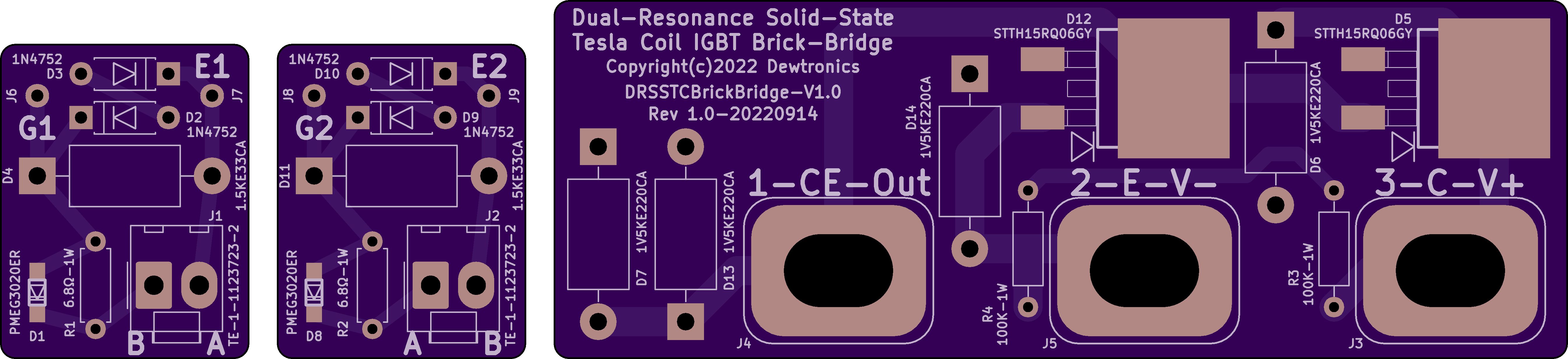
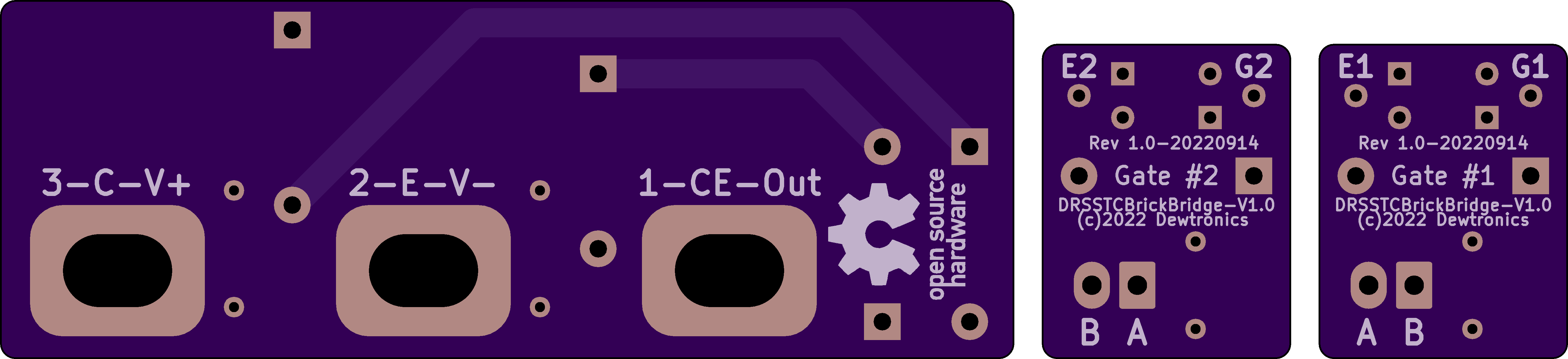
2 layer board of 5.38 x 1.23 inches (136.6 x 31.1 mm)
Uploaded:
September 16, 2022
Shared:
September 16, 2022
Total Price:
$32.95
Dual Resonance Solid-State Tesla Coil IGBT Brick Bridge Support. This provides the TVS clamping and gate buffering logic of the DRSSTC Bridge V2.1, but designed to mount on an IGBT Brick.
Dual Resonance Solid-State Tesla Coil IGBT Brick Bridge Support. This provides the TVS clamping and gate buffering logic of the DRSSTC Bridge V2.1, but designed to mount on an IGBT Brick.
DRSSTC Driver Bridge UCC37322D V1
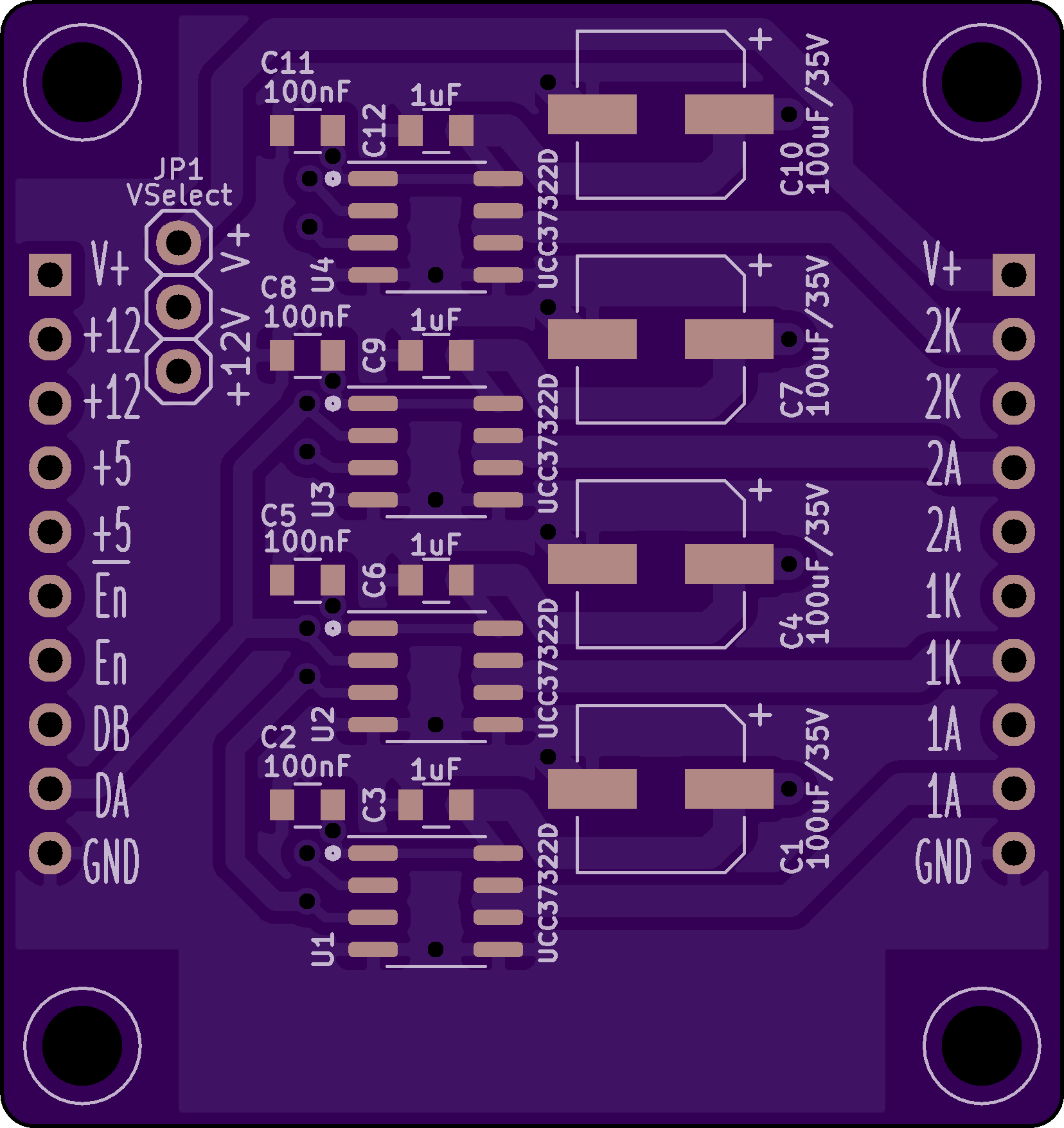
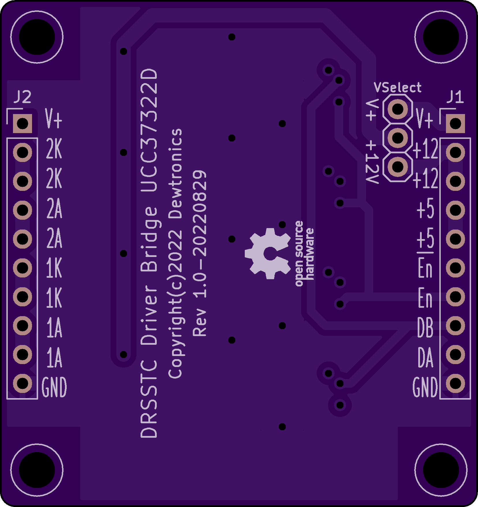
2 layer board of 1.65 x 1.75 inches (41.9 x 44.4 mm)
Uploaded:
September 16, 2022
Shared:
September 16, 2022
Total Price:
$14.40
UCC37322D DRSSTC Driver Bridge daughter board for the DRSSTCDriver-V3.2.
UCC37322D DRSSTC Driver Bridge daughter board for the DRSSTCDriver-V3.2.
DRSSTC Data Acquisition Board V2
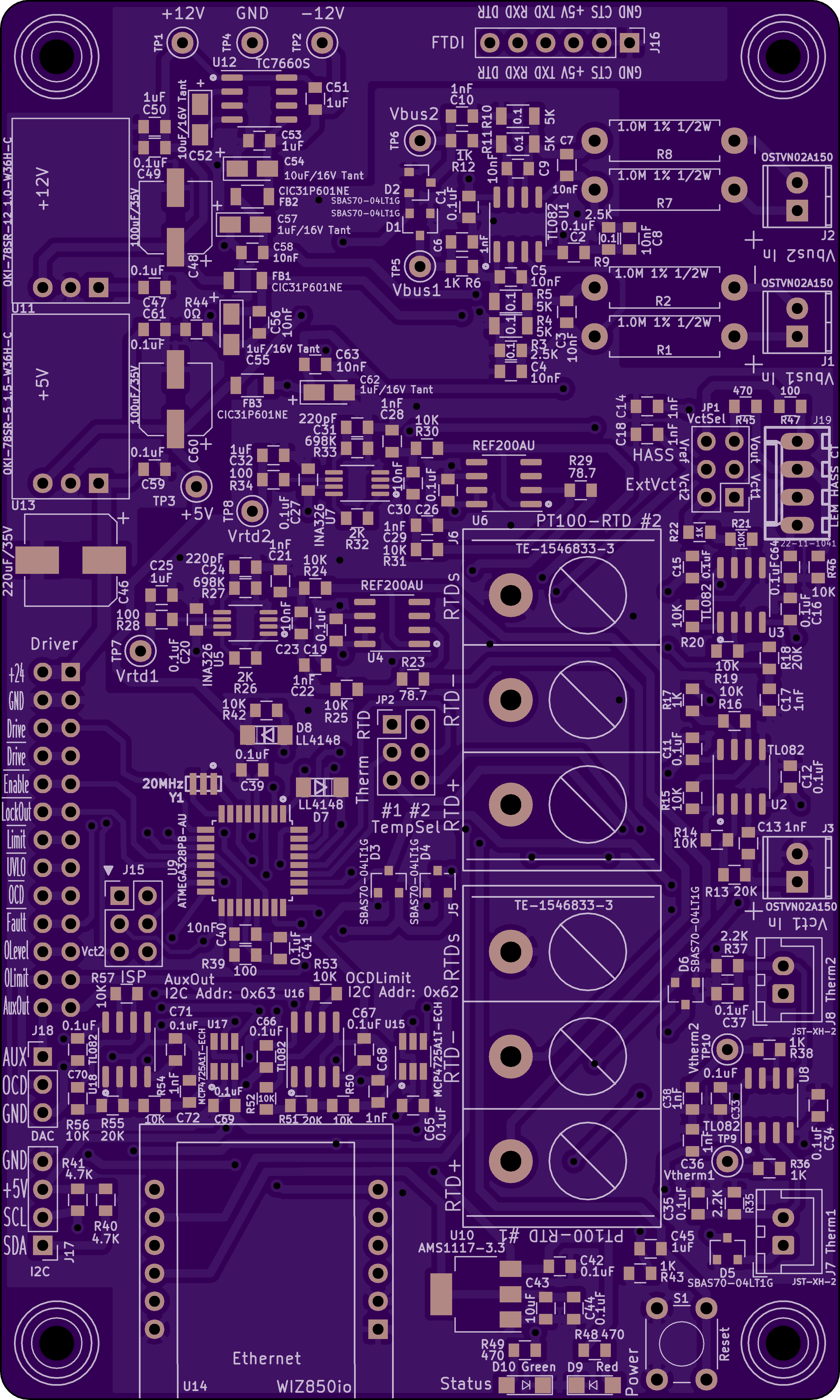
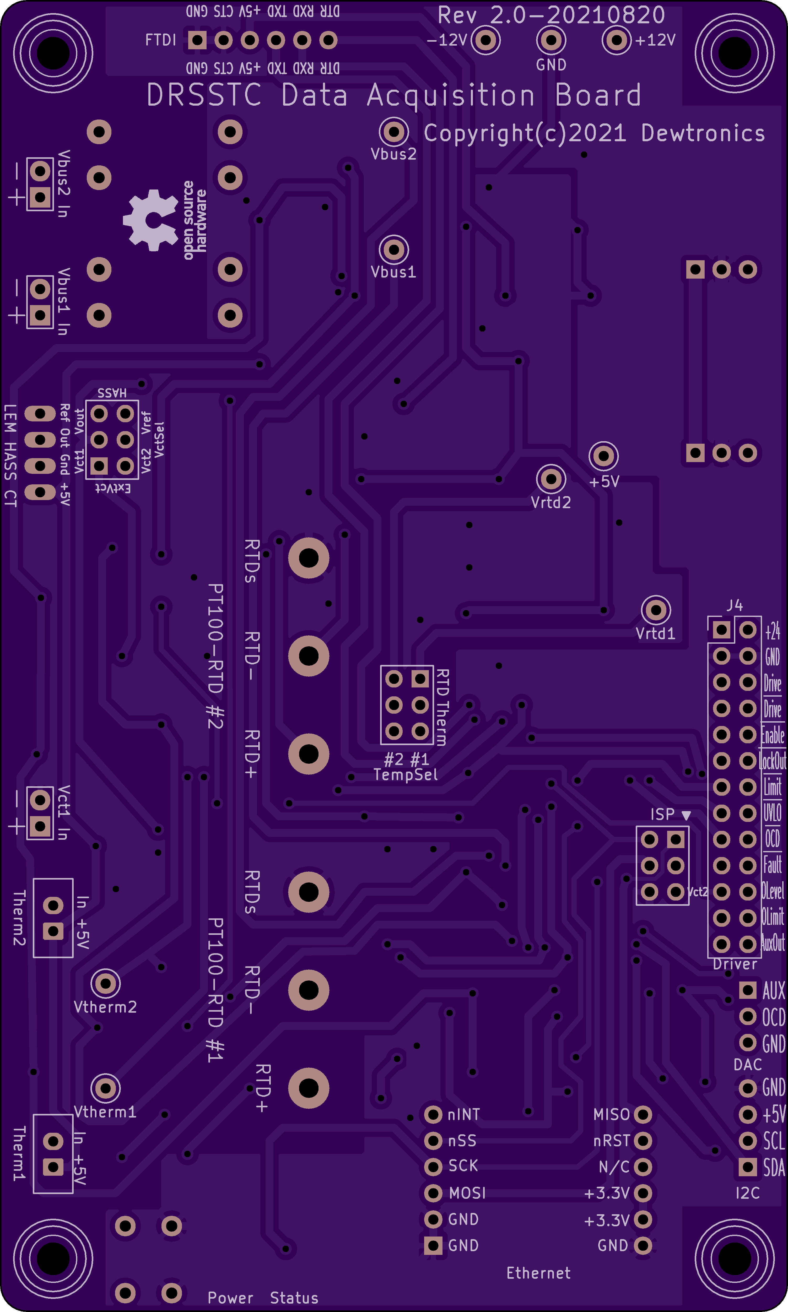
2 layer board of 3.00 x 5.00 inches (76.2 x 127.0 mm)
Uploaded:
August 25, 2021
Shared:
August 25, 2021
Total Price:
$75.00
DRSSTC Data Acquisition Board for DRSSTCDriver-V3.2 designed as a modular stacked pair. This board is a successor to the DRSSTCDAQ-V1 board.
DRSSTC Data Acquisition Board for DRSSTCDriver-V3.2 designed as a modular stacked pair. This board is a successor to the DRSSTCDAQ-V1 board.
DRSSTC Driver Bridge UCC37322 V1
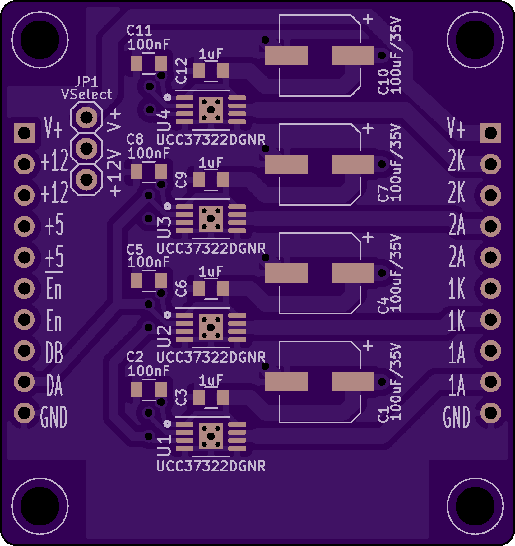
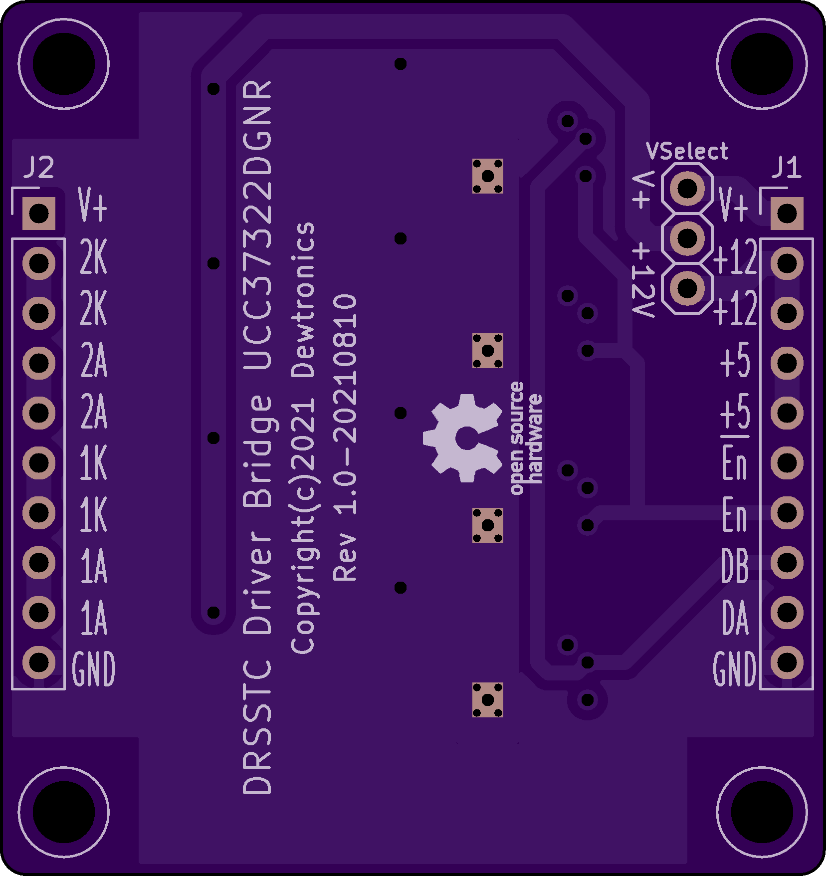
2 layer board of 1.65 x 1.75 inches (41.9 x 44.4 mm)
Uploaded:
August 25, 2021
Shared:
August 25, 2021
Total Price:
$14.40
UCC37322DGNR DRSSTC Driver Bridge daughter board for the DRSSTCDriver-V3.2.
UCC37322DGNR DRSSTC Driver Bridge daughter board for the DRSSTCDriver-V3.2.
DRSSTC Driver Bridge FDD8424H V1
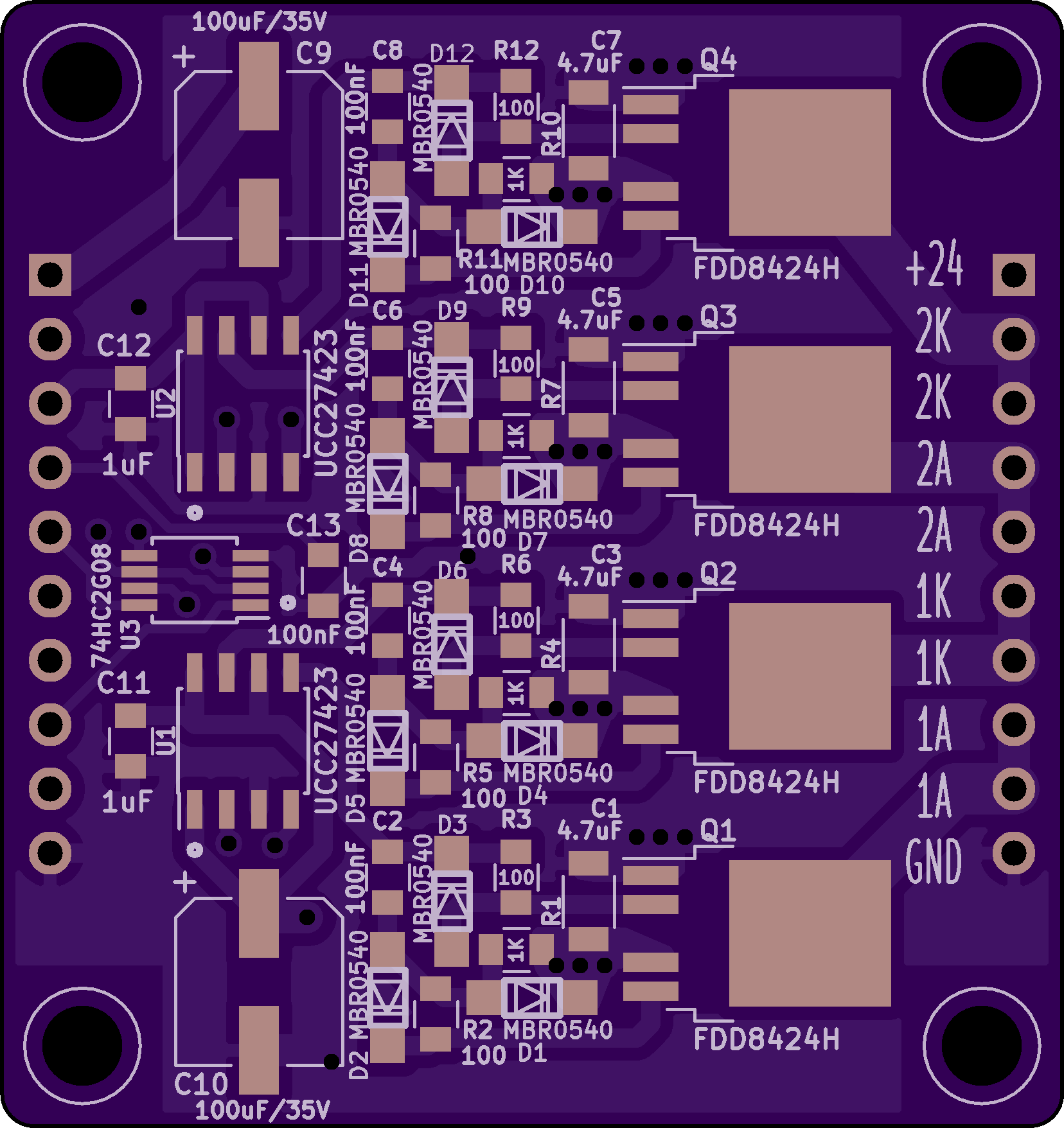
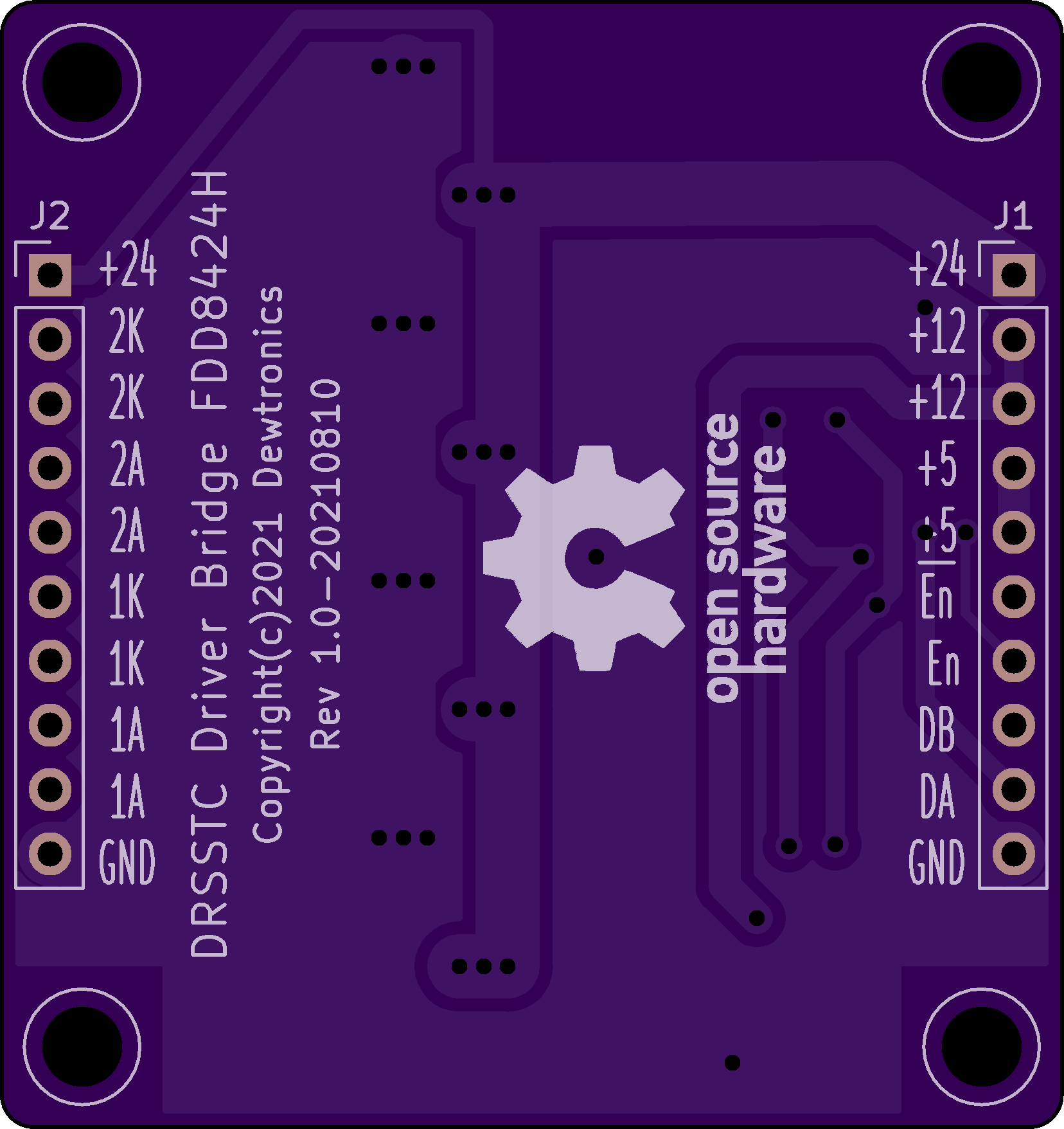
2 layer board of 1.65 x 1.75 inches (41.9 x 44.4 mm)
Uploaded:
August 25, 2021
Shared:
August 25, 2021
Total Price:
$14.40
FDD8424H DRSSTC Driver Bridge daughter board for the DRSSTCDriver-V3.2.
FDD8424H DRSSTC Driver Bridge daughter board for the DRSSTCDriver-V3.2.
