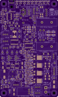
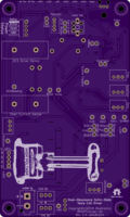
Dual Resonance Solid-State Tesla Coil Driver V2
author: dewhisna
2 layer board of 3.01 x 5.01 inches (76.4 x 127.2 mm)
Uploaded:
December 24, 2018
Shared:
March 01, 2019
Total Price:
$75.20
Do NOT Build This Board It has been replaced by the DRSSTC Driver V2.1.
Driver board for a Dual-Resonance Solid-State Musical Tesla Coil. This version replaces the older V1 version. This design features a zero-current-switching phase-lead circuit, an over-current detection/lockout circuit, an under-voltage lockout circuit, and a PLL-based adjustable dead-time delay. Requires regulated 24VDC power supply. And is designed to be used with either the original DRSSTC Full Bridge Board or the DRSSTC V2 Bridge Board with the DRSSTC Bus Supply V1.
This board adds an interface for a thermal (or other) shutdown (See the DRSSTC Thermal Limiter Board V1 ). It also replaces the UCC37322 driver chips, which kept frying on the V1 board, with UCC27424 driven FDD8424H push-pull MOSFET pairs for driving the gate-drive transformers, allowing for much higher current gate drive. And, this board also supports “skip pulse” (or specifically “skip IGBT drive cycle”) mode in addition to the “skip interrupter” mode typically used. This allows harder driving to the over-current detector threshold.
ERRATA:
1) Resistor R45, which is the current-limiter setting for the on-board +12volt switching power supply, should be 0.2-ohm 1/2W instead of 1-ohm 1/2W. That will allow a full 750mA output from the +12v supply instead of being limited to 150mA, which wasn’t even enough to drive the cooling fan (which needs around 370mA).
2) Similarly, diode D35, in that switching supply circuit, should not be a MBR0540, which is only rated for 500mA. Instead, it should be at least a 1A part, or preferably a PMEG3020ER,115 Schottky diode, which is rated at 2A and has a very low Vf of 365mV for improved efficiency, and is a drop-in replacement for the originally spec’d part.
3) There is a logic error in the lockout circuit that causes a race-condition with the U9 flip-flop (74LVC1G74) between the fiber-optic edge detect signal on the set-input and the main fiber-optic signal on the clock pin. This can cause the system to never start and results in only a short burst of output at the beginning of each interrupter pulse, and it also prevents the skip-pulse mode from working at all.
To resolve, the fiber optic input signal needs to be removed from pin 1 of U9. And the skip-pulse signal on pin 2 needs to move to pin 1. And pin 2 needs to get tied to +5v. To do this, cut the trace leading into pin 1 of U9 (leaving the 90-degree junction intact where it runs under U4), and cut the trace leading into pin 2 of U9 between U9 and resistor R52. Solder a jumper between pin 1 of U9 and R52, on the end where the trace to pin 2 was cut (this takes care of moving the skip-pulse signal from pin 2 to pin 1). And solder a small jumper wire to pin 2 of U9 that runs to +5v. The closest and probably most convenient point for +5v is the far end of capacitor C40, which is the power decoupling capacitor for U9. This jumper can be quite tricky as it has to solder to a single pin on a TSSOP package (0.65mm pin-spacing).
4) Do NOT enable the PLL mode unless you swap U11 and U12 from the non-inverting UCC27424 to the inverting UCC27423 part. Since the FDD8424H output driver transistors invert the output from these chips, if the SG3525 is used with the non-inverting UCC27424, then the dead-time from SG3525 will be converted into intentional overlap between the high-side and low-side of the bridge and you’ll blow the bridge off the board faster than you can blink!! Another alternative might be to use the SG3527 for U3 instead of the SG3525, but it might be difficult to locate since the SG3527 is obsolete.
5) Since the high-side of the FDD8424H circuit is only a momentarily triggered (AC Coupled) state, the disabled state for U11 and U12 need to be high to keep the low-side of the FDD8424H parts activated. However, the enable pin on the UCC27424 sets the outputs low when disabling the output. This will cause a momentary trigger of the FDD8424H to high and then go high impedance when disabling the output. This means the gates of the bridge will be left in a floating state and can possibly turn on unintentionally. The fix for this is to not use the enable inputs of U11 and U12 (pins 1 and 8) at all and instead tie them high (or use UCC27323 parts instead which have no enable signal). Then, add ‘AND’ gates to ‘AND’ the enable output pin 5 of U6 (74LVC1G74) with the ‘Direct’ and ‘~Direct’ outputs of U1 (TL3116 pins 7 and 8) to make the input signals to U11 and U12, via JP2 and JP3, instead of just using ‘Direct’ and ‘~Direct’ only. And switch to the inverting UCC27423 (or UCC27323), which also fixes Errata Item #4. This one is pretty much a showstopper for this board, as it would require extensive surgery to fix. Therefore, it’s recommended that you Do Not Build This Board .
This errata has been resolved in DRSSTC Driver V2.1.

