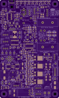
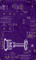
Dual Resonance Solid-State Tesla Coil Driver V2.1
author: dewhisna
2 layer board of 3.01 x 5.01 inches (76.4 x 127.2 mm)
Uploaded:
November 08, 2019
Shared:
November 08, 2019
Total Price:
$75.20
Driver board for a Dual-Resonance Solid-State Musical Tesla Coil. This version replaces the old V2 version, fixing its many errata. This design features a zero-current-switching phase-lead circuit, an over-current detection/lockout circuit, an under-voltage lockout circuit, and a PLL-based adjustable dead-time delay. Requires regulated 24VDC power supply. And is designed to be used with the DRSSTC V2.1 Bridge Board and the DRSSTC Bus Supply V2.
This board adds an interface for a thermal (or other) shutdown (See the DRSSTC Thermal Limiter Board V1 ). It also replaces the UCC37322 driver chips on the V1 board with UCC27423 driven FDD8424H push-pull MOSFET pairs for driving the gate-drive transformers, allowing for much higher current gate drive. And, this board also supports “skip pulse” (or specifically “skip IGBT drive cycle”) mode in addition to the “skip interrupter” mode typically used. This allows harder driving to the over-current detector threshold.
Note: Change RV2 and/or R20 to adjust the SG3525 PLL circuit for your coil’s resonant frequency. With the values of 2K for RV2 and 1K for R20, as labeled, it works for a coil with an approximate resonant frequency of 200-250kHz. Changing them, for example, to 10K for RV2 and 6.8K for R20, it works for a coil that’s approximately 45-100kHz. The exact range is dependent on the dead-time setting, as it alters the frequency slightly, and by component tolerance and circuit parasitics. Refer to the SG3525 datasheet for the frequency equations. Note that FreqOut is 2x the resonant frequency due to the SG3525 dividing the frequency for the dual outputs. The Free-Running frequency of the PLL should be set to about 5% less than 2x the primary circuit resonant.
ERRATA:
1) The outputs from the SG3525 PLL U3 do not feed through the U16 ‘AND’ circuit that merges the ‘Enable’ signal for the output. That means, that on PLL mode, nothing will ever disable the output drive!! That includes both incoming interrupter signal and things like the OCD and UVLO circuits! The simple solution fix is to lift pin 10 of U3 (the SG3525 PLL), which is the ‘shutdown’ pin, so that it’s no longer tied to GND and tie that pin to pin 3 of U6 (the 74LVC1G74 flip/flop), which is the ‘~Enable’ signal. This will shutdown the SG3525 PLL during disable periods (the internal circuit of the PLL is essentially identical to that of the U16 ‘AND’ circuit in this regard).
However, this necessary fix will make it difficult to tune/calibrate the dead-time between the PLL1 and PLL2 outputs of the SG3525, since those outputs will be inherently off most of the time. The “best” bench calibration procedure appears to be to first install the Interrupter Reset Disable jumper and then trigger the fiber optic input with an external light pulse from an interrupter with NO feedback drive into the T1 current transformer (which will keep the ‘Direct’ output of comparator U1, TL3116, deactive). This will release the driver from its initial start-up “lock-out” mode and will keep the lack of interrupter signal from resetting the enable.
Then, use a test-jumper to temporarily short the Anode of D37 (1N4148) and its parallel 1.8K pull-up resistor R50 to ground. That will cause the U6 (74LVC1G74 flip/flop) to set (enter ‘enable’ mode) as if an incoming pulse is seen and will output a low on its pin 3, which will disengage the ‘shutdown’ on the SG3525 (via the newly added jumper) and allow the dead-time between the two outputs to be adjusted. The PLL will then stay running, long enough to calibrate the dead-time adjustment, until something triggers ‘Limit’ or causes a pulse on the ‘Direct’ feedback loop or the Interrupter Reset Disable Jumper is removed, all of which will deactivate the enable.

