Shared Projects by SyncChannelBlog
Shared Projects by SyncChannelBlog
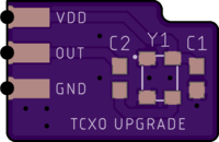
(tr)uSDX TCXO Upgrade
2 layer board of 0.59 x 0.39 inches (15.0 x 10.0 mm)
Uploaded:
August 14, 2022
Shared:
August 14, 2022
Total Price:
$1.15
🔴 I recommend ordering this board with the 2 Layer 2oz 0.8mm "Half Height" Service. 🔴
This PCB allows you to upgrade the (tr)uSDX HF radio with a Temperature Compensated Crystal Oscillator (TCXO) for improved frequency accuracy and stability. The (tr)uSDX uses a standard 27 MHz crystal for…
🔴 I recommend ordering this board with the 2 Layer 2oz 0.8mm “Half Height” Service. 🔴
This PCB allows you to upgrade the (tr)uSDX HF radio with a Temperature Compensated Crystal Oscillator (TCXO) for improved frequency accuracy and stability. The (tr)uSDX uses a standard 27 MHz crystal for frequency synthesis and has no provision on the main board for upgrading with a TCXO. This board adheres to the main board and connects to three pads to power the TCXO and provide the new clock signal to the PLL chip.
Please be aware that assembling and installing this board involves fine SMD soldering and removing the stock crystal from the main board in the radio. Removing the crystal involves some small risk of damaging the board just like removing any part, and damaging the PLL circuit would render the radio inoperable. Proceed with caution if you decide to perform this mod.
This mod is not “official” in any way or associated with the (tr)uSDX project, other than that I am a user of the radio and wanted to contribute a useful mod that I developed to the community.
Parts List:
Note: I have tested the TCXO above so I know it works, but you should be able to substitute other 27 MHz TCXOs that have a 3.20mm x 2.50mm package and operate on 3.3V.
Board Files:
Eagle files are available on GitHub: (truSDX-TCXO-Upgrade)
The PCB uploaded here on OSHPark is Rev B of the PCB. Rev A was an early version of the board that I made for testing. There is no reason to order it instead, but I have included it in the GitHub repo in case someone wants it.
Assembly:
Assembly of this board is straightforward if you are comfortable soldering very small SMD components. Please do watch the orientation of the TCXO. There is a small dot on the PCB to indicate pin 1.

Testing the Board:
If possible, test the board after assembly to make sure the TCXO is oscillating correctly before installing it in the radio. Ideally the waveform should be verified on an oscilloscope and the frequency measured with a counter. The waveform from the ECS TCXO is a ~1.2 Vpp clipped sine wave and the frequency should be 27.000000 MHz +/- 54 Hz (2 ppm).
Install Photos:
Installation requires the removal of the stock 27 MHz crystal, Y1, from the main board. A hot air gun is the most common way to do this, but please be careful that you do not disturb or blow off any neighboring parts. I personally used ChipQuik instead. Removing the crystal frees up pads for the TCXO output connection and ground. VDD is obtained from one end of diode D2 which is next to the crystal footprint as shown.

Next, test fit the TCXO board on the main board. You need to line up the three castellations/pads for VDD, OUT and GND with the three pads on the main board shown above. The castellations should be directly over the pads or set back slightly to allow access for soldering.
There is unfortunately no where to screw down or otherwise secure the TCXO board to the main board, so it will need to be adhered in some way. I made the board big enough that it overlaps with nearby chips and parts, so there is plenty of surface area to use glue or double sided tape. I used a piece of double sided tape that covered almost the entire underside of the TCXO board, and it makes good contact with U6, U3, D1 and D2. You could further use some epoxy, hot melt glue, and/or kapton tape to secure the board.

Now you need to make a connection between VDD, OUT and GND on the TCXO board and the respective pads below. I used small tinned wire to do this. With a long piece of wire in hand, lay it vertically in the castellation and extending down to touch the pad. Solder the end of the wire to the pad on the main board, then trim the wire flush with the top of the TCXO board, then solder the wire into the castellation and/or on the pad.
The castellated vias are spaced 0.1"/2.54mm apart, so you could theoretically use standard pin header instead of tinned wire. However, you will need to trim the pins very short to keep the height of the TCXO board to a minimum. It might not be clear in the zoomed in pictures, but the space between the mod board and the main board is very small. I think tinned wire as shown is the best way to make the connection, but you may find some more creative approach.

With the TCXO mod installed, re-assemble the radio and test it to make sure you can change frequencies and receive and transmit. If you had previously performed a frequency calibration and changed the value of setting 8.3 Ref freq, you will want to reset this to 27000000. TCXOs aren’t perfect, and based on the exact oscillation frequency of yours you may find that a setting of 27000050 or 26999950 is more accurate. Either way, it should be much more accurate than the default crystal.
I have performed this mod on two of my (tr)uSDX radios with good results. Good luck if you decide to attempt the mod yourself!
Show full description
🔴 I recommend ordering this board with the 2 Layer 2oz 0.8mm "Half Height" Service. 🔴
This PCB allows you to upgrade the (tr)uSDX HF radio with a Temperature Compensated Crystal Oscillator (TCXO) for improved frequency accuracy and stability. The (tr)uSDX uses a standard 27 MHz crystal for…
🔴 I recommend ordering this board with the 2 Layer 2oz 0.8mm “Half Height” Service. 🔴
This PCB allows you to upgrade the (tr)uSDX HF radio with a Temperature Compensated Crystal Oscillator (TCXO) for improved frequency accuracy and stability. The (tr)uSDX uses a standard 27 MHz crystal for frequency synthesis and has no provision on the main board for upgrading with a TCXO. This board adheres to the main board and connects to three pads to power the TCXO and provide the new clock signal to the PLL chip.
Please be aware that assembling and installing this board involves fine SMD soldering and removing the stock crystal from the main board in the radio. Removing the crystal involves some small risk of damaging the board just like removing any part, and damaging the PLL circuit would render the radio inoperable. Proceed with caution if you decide to perform this mod.
This mod is not “official” in any way or associated with the (tr)uSDX project, other than that I am a user of the radio and wanted to contribute a useful mod that I developed to the community.
Parts List:
Note: I have tested the TCXO above so I know it works, but you should be able to substitute other 27 MHz TCXOs that have a 3.20mm x 2.50mm package and operate on 3.3V.
Board Files:
Eagle files are available on GitHub: (truSDX-TCXO-Upgrade)
The PCB uploaded here on OSHPark is Rev B of the PCB. Rev A was an early version of the board that I made for testing. There is no reason to order it instead, but I have included it in the GitHub repo in case someone wants it.
Assembly:
Assembly of this board is straightforward if you are comfortable soldering very small SMD components. Please do watch the orientation of the TCXO. There is a small dot on the PCB to indicate pin 1.

Testing the Board:
If possible, test the board after assembly to make sure the TCXO is oscillating correctly before installing it in the radio. Ideally the waveform should be verified on an oscilloscope and the frequency measured with a counter. The waveform from the ECS TCXO is a ~1.2 Vpp clipped sine wave and the frequency should be 27.000000 MHz +/- 54 Hz (2 ppm).
Install Photos:
Installation requires the removal of the stock 27 MHz crystal, Y1, from the main board. A hot air gun is the most common way to do this, but please be careful that you do not disturb or blow off any neighboring parts. I personally used ChipQuik instead. Removing the crystal frees up pads for the TCXO output connection and ground. VDD is obtained from one end of diode D2 which is next to the crystal footprint as shown.

Next, test fit the TCXO board on the main board. You need to line up the three castellations/pads for VDD, OUT and GND with the three pads on the main board shown above. The castellations should be directly over the pads or set back slightly to allow access for soldering.
There is unfortunately no where to screw down or otherwise secure the TCXO board to the main board, so it will need to be adhered in some way. I made the board big enough that it overlaps with nearby chips and parts, so there is plenty of surface area to use glue or double sided tape. I used a piece of double sided tape that covered almost the entire underside of the TCXO board, and it makes good contact with U6, U3, D1 and D2. You could further use some epoxy, hot melt glue, and/or kapton tape to secure the board.

Now you need to make a connection between VDD, OUT and GND on the TCXO board and the respective pads below. I used small tinned wire to do this. With a long piece of wire in hand, lay it vertically in the castellation and extending down to touch the pad. Solder the end of the wire to the pad on the main board, then trim the wire flush with the top of the TCXO board, then solder the wire into the castellation and/or on the pad.
The castellated vias are spaced 0.1"/2.54mm apart, so you could theoretically use standard pin header instead of tinned wire. However, you will need to trim the pins very short to keep the height of the TCXO board to a minimum. It might not be clear in the zoomed in pictures, but the space between the mod board and the main board is very small. I think tinned wire as shown is the best way to make the connection, but you may find some more creative approach.

With the TCXO mod installed, re-assemble the radio and test it to make sure you can change frequencies and receive and transmit. If you had previously performed a frequency calibration and changed the value of setting 8.3 Ref freq, you will want to reset this to 27000000. TCXOs aren’t perfect, and based on the exact oscillation frequency of yours you may find that a setting of 27000050 or 26999950 is more accurate. Either way, it should be much more accurate than the default crystal.
I have performed this mod on two of my (tr)uSDX radios with good results. Good luck if you decide to attempt the mod yourself!
Show full description
-
Actions
- Order Board
- Download
- Permalink
- Embed link
Ordering shared project
Hey there! Before ordering, make sure you have all the info you need to complete and use this design. This usually means a component list, and sometimes additional information such as assembly notes, source code, or usage guides.Since this is a project designed by a community member, it may contain design errors that prevent it from working as intended. OSH Park cannot place any guarantees about the functionality or correctness of the design.
MX-P50M Keyer Mod
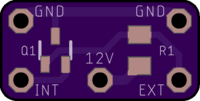
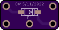
2 layer board of 0.50 x 0.25 inches (12.7 x 6.4 mm)
Uploaded:
June 01, 2022
Shared:
June 02, 2022
Total Price:
$0.60
Tiny PCB (0.5"x0.25") for modifying the MX-P50M HF amplifier with an upgraded keyer circuit. The circuit is added in-line on the keying wire to buffer the signal from the radio and add a flyback diode across the transmit relay, greatly improving safety for the radio itself.
This mod was create…
Tiny PCB (0.5"x0.25") for modifying the MX-P50M HF amplifier with an upgraded keyer circuit. The circuit is added in-line on the keying wire to buffer the signal from the radio and add a flyback diode across the transmit relay, greatly improving safety for the radio itself.
This mod was created by Kevin Loughin KB9RLW, please see his excellent YouTube video here where he describes the circuit, the theory of operation and the justification for adding it to the amp: Ham Radio - Modifying the MX-P50M amplifier to fix keying and installing it to my desk.. All credit goes to him for the original mod. You should also check out this video by Mike K8MRD where he demonstrates performing the mod on his own amp and installing the circuit: MX-P50M Keyer Mod and Installation for Icom 705. While it’s very possible to build the circuit with through-hole components as shown in both videos, I decided to make a small PCB with surface mount components to create a cleaner finished product for the mod.
Parts List:
- Q1: MMST5401-7-F PNP Transistor SOT323 (Digikey)
- D1: 1N4148 Diode SOD123 (Digikey)
- R1: 10k 0805 Resistor (Digikey)
Assembly:
Assembly of this board is straightforward if you are comfortable soldering very small SMD components. All three components on the PCB have different footprints, so there is little risk of installing a part in the wrong spot. Please do watch the polarity of the diode. The stripe on the body of the diode lines up with the stripe on the PCB.
Testing the Board:
It is possible to test your assembled board after soldering the components and before installing it inside of your amplifier. You will need an LED and a resistor of about 1k ohm. Through hole components are fine and a breadboard would help with this to quickly assemble the test circuit and provide a place to connect your hookup wires. I personally connected the LED and resistor on a breadboard along with the supply voltage, used jumper wires coming off of the breadboard and just jammed them into the holes of the PCB and held everything together with my fingers for the few seconds it took to conduct the test.
- Connect the Anode (positive) side of the LED to some supply voltage, anything from 5-15V is fine. You could use a 9V battery, 12V from a radio battery, etc.
- Connect the Cathode (negative) side of the LED to one end of the resistor, and connect the other end of the resistor to the INT hole on the mod PCB.
- Connect the same supply voltage you used on the LED to the 12V hole on the mod PCB, and also connect one of the GND holes on the PCB to the ground of the supply.
- At this point the mod circuit is active and the LED should be OFF.
- Connect a wire to the EXT hole on the mod PCB and touch it to the ground of the supply. The LED should turn ON. As soon as you remove the wire from ground, the LED should turn back OFF. This replicates the SEND line from the radio dropping low during transmit.
That’s it. Use an LED with a current limiting resistor as a load hooked up to the emitter of the PNP transistor, and ensure that the transistor turns on when the base is pulled to ground to sink current through the LED.
Install Photos:
The board is designed to be easily inserted in-line on the keying wire inside of the MX-P50M amplifier. The PCB is shown here assembled with the SMD components that implement the mod circuit in KB9RLW’s video.

Cut the keying wires (smaller red and black wires) inside of the amplifier approximately half way between the case and the white connector that goes to the amp internally. Strip a small amount of insulation off the ends of each wire. As you see here, the mod PCB is designed with holes on the corners for the four wire ends that you just prepped. The side of the red wire that goes to the outside of the amp and the radio is soldered to EXT, the side of the red wire that goes to the PCB of the amplifier is soldered to INT, and the two ends of the black ground wire are soldered to the GND holes.

Here the board is soldered to the red and black keying wires. I decided to insert the wires into the holes from the underside to create a neater final install that would sit nicely inside of the amplifier.

Next solder a small gauge wire to the 12V hole on the mod PCB. Eight inches of 16 gauge wire or so should work. I once again inserted the wire from the underside of the board as shown. Once this wire is soldered, you can clean the flux residue off of the mod PCB if you desire with some flux cleaner or isopropyl alcohol.

Now you should apply some heat shrink over the mod PCB to seal things up and help to prevent shorts. 3/8" 3:1 heat shrink worked for me. With that applied, you can reconnect the white connector on the keying wire to the circuit board of the amp and start to tuck the mod circuit down into the case of the amplifier behind the relays.

Finally, solder the 12V wire from the mod circuit to the amplifier board on the same pad where the main incoming supply (larger red wire) goes. Tiddy things up inside of the case, re-install the bottom cover and test the amplifier.

This mod works great in my amplifier, and I’m happy to know that the mod circuit is just as robust and reliable as the rest of the circuitry inside of the amp. Good luck with the mod if you decide to try it yourself.
Show full description
Tiny PCB (0.5"x0.25") for modifying the MX-P50M HF amplifier with an upgraded keyer circuit. The circuit is added in-line on the keying wire to buffer the signal from the radio and add a flyback diode across the transmit relay, greatly improving safety for the radio itself.
This mod was create…
Tiny PCB (0.5"x0.25") for modifying the MX-P50M HF amplifier with an upgraded keyer circuit. The circuit is added in-line on the keying wire to buffer the signal from the radio and add a flyback diode across the transmit relay, greatly improving safety for the radio itself.
This mod was created by Kevin Loughin KB9RLW, please see his excellent YouTube video here where he describes the circuit, the theory of operation and the justification for adding it to the amp: Ham Radio - Modifying the MX-P50M amplifier to fix keying and installing it to my desk.. All credit goes to him for the original mod. You should also check out this video by Mike K8MRD where he demonstrates performing the mod on his own amp and installing the circuit: MX-P50M Keyer Mod and Installation for Icom 705. While it’s very possible to build the circuit with through-hole components as shown in both videos, I decided to make a small PCB with surface mount components to create a cleaner finished product for the mod.
Parts List:
- Q1: MMST5401-7-F PNP Transistor SOT323 (Digikey)
- D1: 1N4148 Diode SOD123 (Digikey)
- R1: 10k 0805 Resistor (Digikey)
Assembly:
Assembly of this board is straightforward if you are comfortable soldering very small SMD components. All three components on the PCB have different footprints, so there is little risk of installing a part in the wrong spot. Please do watch the polarity of the diode. The stripe on the body of the diode lines up with the stripe on the PCB.
Testing the Board:
It is possible to test your assembled board after soldering the components and before installing it inside of your amplifier. You will need an LED and a resistor of about 1k ohm. Through hole components are fine and a breadboard would help with this to quickly assemble the test circuit and provide a place to connect your hookup wires. I personally connected the LED and resistor on a breadboard along with the supply voltage, used jumper wires coming off of the breadboard and just jammed them into the holes of the PCB and held everything together with my fingers for the few seconds it took to conduct the test.
- Connect the Anode (positive) side of the LED to some supply voltage, anything from 5-15V is fine. You could use a 9V battery, 12V from a radio battery, etc.
- Connect the Cathode (negative) side of the LED to one end of the resistor, and connect the other end of the resistor to the INT hole on the mod PCB.
- Connect the same supply voltage you used on the LED to the 12V hole on the mod PCB, and also connect one of the GND holes on the PCB to the ground of the supply.
- At this point the mod circuit is active and the LED should be OFF.
- Connect a wire to the EXT hole on the mod PCB and touch it to the ground of the supply. The LED should turn ON. As soon as you remove the wire from ground, the LED should turn back OFF. This replicates the SEND line from the radio dropping low during transmit.
That’s it. Use an LED with a current limiting resistor as a load hooked up to the emitter of the PNP transistor, and ensure that the transistor turns on when the base is pulled to ground to sink current through the LED.
Install Photos:
The board is designed to be easily inserted in-line on the keying wire inside of the MX-P50M amplifier. The PCB is shown here assembled with the SMD components that implement the mod circuit in KB9RLW’s video.

Cut the keying wires (smaller red and black wires) inside of the amplifier approximately half way between the case and the white connector that goes to the amp internally. Strip a small amount of insulation off the ends of each wire. As you see here, the mod PCB is designed with holes on the corners for the four wire ends that you just prepped. The side of the red wire that goes to the outside of the amp and the radio is soldered to EXT, the side of the red wire that goes to the PCB of the amplifier is soldered to INT, and the two ends of the black ground wire are soldered to the GND holes.

Here the board is soldered to the red and black keying wires. I decided to insert the wires into the holes from the underside to create a neater final install that would sit nicely inside of the amplifier.

Next solder a small gauge wire to the 12V hole on the mod PCB. Eight inches of 16 gauge wire or so should work. I once again inserted the wire from the underside of the board as shown. Once this wire is soldered, you can clean the flux residue off of the mod PCB if you desire with some flux cleaner or isopropyl alcohol.

Now you should apply some heat shrink over the mod PCB to seal things up and help to prevent shorts. 3/8" 3:1 heat shrink worked for me. With that applied, you can reconnect the white connector on the keying wire to the circuit board of the amp and start to tuck the mod circuit down into the case of the amplifier behind the relays.

Finally, solder the 12V wire from the mod circuit to the amplifier board on the same pad where the main incoming supply (larger red wire) goes. Tiddy things up inside of the case, re-install the bottom cover and test the amplifier.

This mod works great in my amplifier, and I’m happy to know that the mod circuit is just as robust and reliable as the rest of the circuitry inside of the amp. Good luck with the mod if you decide to try it yourself.
Show full description
-
Actions
- Order Board
- Download
- Permalink
- Embed link
Ordering shared project
Hey there! Before ordering, make sure you have all the info you need to complete and use this design. This usually means a component list, and sometimes additional information such as assembly notes, source code, or usage guides.Since this is a project designed by a community member, it may contain design errors that prevent it from working as intended. OSH Park cannot place any guarantees about the functionality or correctness of the design.
QRP Antenna Trap
2 layer board of 1.00 x 0.25 inches (25.4 x 6.4 mm)
Uploaded:
March 15, 2022
Shared:
March 15, 2022
Total Price:
$1.25
Tiny PCB (1"x0.25") for making QRP HF antenna traps. The board allows easy soldering of the inductor, SMD capacitor (0805 or 0603) and antenna wires and also provides strain relief holes for the wires. Please see the excellent YouTube video by Adam K6ARK: [HF Antenna Micro-Traps - DIY Build Proje…
Tiny PCB (1"x0.25") for making QRP HF antenna traps. The board allows easy soldering of the inductor, SMD capacitor (0805 or 0603) and antenna wires and also provides strain relief holes for the wires. Please see the excellent YouTube video by Adam K6ARK: HF Antenna Micro-Traps - DIY Build Project. This PCB is a replacement for the proto-board that he uses in the video and should make assembly of the traps a little easier. Adam listed out the materials you need in the video description with links.

Notes:
You must use the larger T50-2 toroid for the board to fit inside of the wound inductor. (0.25" is the minimum PCB height/width so I couldn’t make it narrower) It’s possible that you could sand the sides of the board down to squeeze it inside of a smaller coil, but I haven’t tried that yet.
I used 26 gauge magnet wire and didn’t have any issues fitting the board inside the inductor, though it is indeed a snug fit.
The board has a spot for a 0805 capacitor on top and a 0603 capacitor on the bottom. Use either one, or use both to put the capacitors in parallel to help you achieve certain values. They are in parallel with the inductor to create the resonant circuit, and extra holes are provided on either side to solder in the antenna wire as shown.
The strain relief holes are large enough to accept Sotabeams lightweight wire and Polystealth wire, two very popular options for making antennas like this. The holes are quite generous so other small gauge wire would work too.
Credit goes to K6ARK for his presentation on micro HF antenna traps. Perhaps this little PCB I made will help you build your own. Enjoy!
Show full description
Tiny PCB (1"x0.25") for making QRP HF antenna traps. The board allows easy soldering of the inductor, SMD capacitor (0805 or 0603) and antenna wires and also provides strain relief holes for the wires. Please see the excellent YouTube video by Adam K6ARK: [HF Antenna Micro-Traps - DIY Build Proje…
Tiny PCB (1"x0.25") for making QRP HF antenna traps. The board allows easy soldering of the inductor, SMD capacitor (0805 or 0603) and antenna wires and also provides strain relief holes for the wires. Please see the excellent YouTube video by Adam K6ARK: HF Antenna Micro-Traps - DIY Build Project. This PCB is a replacement for the proto-board that he uses in the video and should make assembly of the traps a little easier. Adam listed out the materials you need in the video description with links.

Notes:
You must use the larger T50-2 toroid for the board to fit inside of the wound inductor. (0.25" is the minimum PCB height/width so I couldn’t make it narrower) It’s possible that you could sand the sides of the board down to squeeze it inside of a smaller coil, but I haven’t tried that yet.
I used 26 gauge magnet wire and didn’t have any issues fitting the board inside the inductor, though it is indeed a snug fit.
The board has a spot for a 0805 capacitor on top and a 0603 capacitor on the bottom. Use either one, or use both to put the capacitors in parallel to help you achieve certain values. They are in parallel with the inductor to create the resonant circuit, and extra holes are provided on either side to solder in the antenna wire as shown.
The strain relief holes are large enough to accept Sotabeams lightweight wire and Polystealth wire, two very popular options for making antennas like this. The holes are quite generous so other small gauge wire would work too.
Credit goes to K6ARK for his presentation on micro HF antenna traps. Perhaps this little PCB I made will help you build your own. Enjoy!
Show full description
-
Actions
- Order Board
- Download
- Permalink
- Embed link
Ordering shared project
Hey there! Before ordering, make sure you have all the info you need to complete and use this design. This usually means a component list, and sometimes additional information such as assembly notes, source code, or usage guides.Since this is a project designed by a community member, it may contain design errors that prevent it from working as intended. OSH Park cannot place any guarantees about the functionality or correctness of the design.
USB to VGA Adapter SMA Breakout
2 layer board of 1.00 x 1.26 inches (25.4 x 32.1 mm)
Uploaded:
May 13, 2018
Shared:
May 13, 2018
Total Price:
$6.30
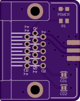
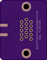
For use with USB to VGA adapters and Osmo-fl2k.
The RED "transmit" pin from the adapter is broken out to an SMA connector. The +5V pin is used to drive an optional power LED. The Cable Detect pins are broken out to solder jumpers to connect them to ground. Cable detect is taken care of in soft…
For use with USB to VGA adapters and Osmo-fl2k.
The RED “transmit” pin from the adapter is broken out to an SMA connector. The +5V pin is used to drive an optional power LED. The Cable Detect pins are broken out to solder jumpers to connect them to ground. Cable detect is taken care of in software so these are not currently needed, but I broke them out just in case.
This board does not provide impedance matching, attenuation or filtering. It is merely an SMA breakout.
Bill of Materials:
- VGA Connector: DSUB HD15 Right Angle (Digikey PN# A31927-ND)
- SMA Connector: Edge launch SMA for .062" PCB (Digikey PN# CON-SMA-EDGE-S-ND)
- Power LED: 0805 (optional)
- R1: 0805 470Ω to 1kΩ (optional)
Show full description
For use with USB to VGA adapters and Osmo-fl2k.
The RED "transmit" pin from the adapter is broken out to an SMA connector. The +5V pin is used to drive an optional power LED. The Cable Detect pins are broken out to solder jumpers to connect them to ground. Cable detect is taken care of in soft…
For use with USB to VGA adapters and Osmo-fl2k.
The RED “transmit” pin from the adapter is broken out to an SMA connector. The +5V pin is used to drive an optional power LED. The Cable Detect pins are broken out to solder jumpers to connect them to ground. Cable detect is taken care of in software so these are not currently needed, but I broke them out just in case.
This board does not provide impedance matching, attenuation or filtering. It is merely an SMA breakout.
Bill of Materials:
- VGA Connector: DSUB HD15 Right Angle (Digikey PN# A31927-ND)
- SMA Connector: Edge launch SMA for .062" PCB (Digikey PN# CON-SMA-EDGE-S-ND)
- Power LED: 0805 (optional)
- R1: 0805 470Ω to 1kΩ (optional)
Show full description
-
Actions
- Order Board
- Download
- Permalink
- Embed link
Ordering shared project
Hey there! Before ordering, make sure you have all the info you need to complete and use this design. This usually means a component list, and sometimes additional information such as assembly notes, source code, or usage guides.Since this is a project designed by a community member, it may contain design errors that prevent it from working as intended. OSH Park cannot place any guarantees about the functionality or correctness of the design.
Z80 Test Circuit
2 layer board of 2.25 x 2.75 inches (57.2 x 69.8 mm)
Uploaded:
September 23, 2017
Shared:
September 23, 2017
Total Price:
$30.90
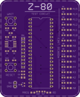
This board implements a classic Z80 microprocessor test circuit. All data pins are pulled low, causing it to execute the NOP instruction $00 repeatedly. The program counter increments and the activity on the address lines is visualized using LEDs. A slow clock signal is applied to make the addres…
This board implements a classic Z80 microprocessor test circuit. All data pins are pulled low, causing it to execute the NOP instruction $00 repeatedly. The program counter increments and the activity on the address lines is visualized using LEDs. A slow clock signal is applied to make the address bus activity slow enough to see.
The MREQ and RD pins are also brought out to LEDs. Push buttons are available for the RESET and WAIT lines. The clock signal is generated using a 555 timer.
The board is powered by applying 5V to the 0.1" header pins. Reverse polarity protection is provided using a P-Channel MOSFET.
This board is mostly a novelty. It’s really cool to see the program counter increment on the address pin LEDs and the MREQ and RD LEDs flash. It is not possible to execute an actual program on this board, as it has exactly one byte of “memory” with the contents $00. :)
BOM
- U1: Zilog Z80 40DIP
- U2: 555 Timer 8SOIC
- Q1: Alpha & Omega AO3401A P-Channel MOSFET SOT-23 or similar
- R1-R19, R21-R22: 1k 0603
- R20: 22k 0603
- C1: 10 uF 0805
- C2, C5: 1 uF 0603
- C3-C4, C6-C7: 100 nF 0603
- RN1: 1k, 8 resistor (9 pin) SIP
- A0-A15, MREQ, RD: 0805 SMD LEDs (colors of your choice)
- RESET and WAIT switches: SPST tactile switch Through hole
- 5V header: 1x2 0.1" standard header pins
Notes
- R20, R21, and C5 set the 555 clock signal frequency. The values provided above will set a clock of approximately 32 Hz. You can use an online 555 calculator to pick different values and adjust the clock frequency as you like. In relation to the classic 555 circuit schematic: R21 on this board = R1, R20 = R2, and C5 = C.
- Brand new Z80 microprocessors are available on Digikey if you don’t have one.
Eagle Files
https://github.com/SyncChannel/Z80-Test-Circuit
Other References
http://www.z80.info/z80test0.htm
https://z80project.wordpress.com/2014/02/09/z80-test-circuit/
Show full description
-
Actions
- Order Board
- Download
- Permalink
- Embed link
Ordering shared project
Hey there! Before ordering, make sure you have all the info you need to complete and use this design. This usually means a component list, and sometimes additional information such as assembly notes, source code, or usage guides.Since this is a project designed by a community member, it may contain design errors that prevent it from working as intended. OSH Park cannot place any guarantees about the functionality or correctness of the design.
- SERVICES
- Upload Your File
- Prototypes
- HELP
- Support
- If you can't find what you're looking for, please contact us at [email protected]
- CONNECT
- Shared Projects
- Log in / Sign up
