SNES 16Mb TSOP-DIP Backside Adapter Rev.E
author: ziggy587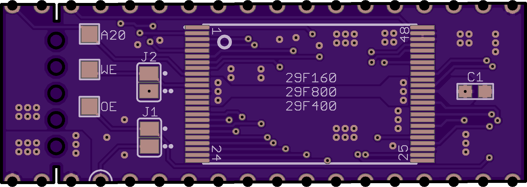
2 layer board of 1.79 x 0.61 inches (45.4 x 15.6 mm)
Uploaded:
February 04, 2025
Shared:
February 04, 2025
Total Price:
$5.45
Rev.E is not tested! So far only Rev.B has been tested with an 8Mb game on a 29F800 in a 32-pin socket, and it was found to work. Use at your own risk!
This adapter installs on the backside of a SNES mask ROM. You must cut or isolate the /OE pin on the mask ROM and tie it to Vcc.
This adapter is made to work on both 32-pin and 36-pin mask ROM sockets. If using on a 32-pin socket, you will most likely have to cut off the 4 pins for clearance. You could score both sides with a utility knife or X-Acto blade and then snap it off, or use small flush cutters.
If you are using a 29F160 on a 32-pin socket, you will have to use a jumper wire for A20.
J1 connects /OE from the mask ROM socket to the TSOP chip. If you are only using a single TSOP chip, then you must close J1. If you leave J1 open, then you can use the /OE solder pad on this adapter to connect the /OE pin of the TSOP to where ever you need it.
J2 Connects TSOP /WE to +5V. Close J2 to put the TSOP into read mode. Alternatively, leave J2 open and connect the WE solder pad to SRAM /WE or cart edge connector.
C1 is for an 0603 0.1µF decoupling capacitor.
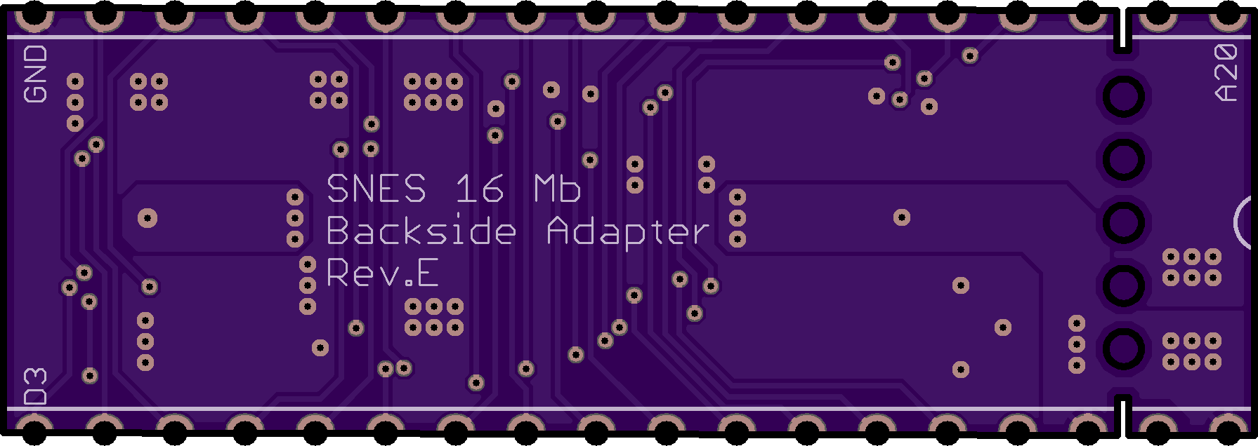
Don’t forget to isolate the bottom of the adapter to prevent shorts.
Revision History:
Rev.E
-Longer TSOP pads, easier to hand solder -Minor trace changes, added more ground vias
Rev.D
-New layout, retraced entire board -Added J2 for write enable signal
Rev.C
-Changed J1 from 0603 to custom jumper pad -Cleaned up some traces and various tolerances -Enlarged silkscreen indicators from 32 to 40 -Added Vcc via to C1 pad, removed extra vias -Moved /OE solder pad, more clearance from surrounding vias
Rev.E is not tested! So far only Rev.B has been tested with an 8Mb game on a 29F800 in a 32-pin socket, and it was found to work. Use at your own risk!
This adapter installs on the backside of a SNES mask ROM. You must cut or isolate the /OE pin on the mask ROM and tie it to Vcc.
This adapter is made to work on both 32-pin and 36-pin mask ROM sockets. If using on a 32-pin socket, you will most likely have to cut off the 4 pins for clearance. You could score both sides with a utility knife or X-Acto blade and then snap it off, or use small flush cutters.
If you are using a 29F160 on a 32-pin socket, you will have to use a jumper wire for A20.
J1 connects /OE from the mask ROM socket to the TSOP chip. If you are only using a single TSOP chip, then you must close J1. If you leave J1 open, then you can use the /OE solder pad on this adapter to connect the /OE pin of the TSOP to where ever you need it.
J2 Connects TSOP /WE to +5V. Close J2 to put the TSOP into read mode. Alternatively, leave J2 open and connect the WE solder pad to SRAM /WE or cart edge connector.
C1 is for an 0603 0.1µF decoupling capacitor.
Don’t forget to isolate the bottom of the adapter to prevent shorts.
Revision History:
Rev.E
-Longer TSOP pads, easier to hand solder -Minor trace changes, added more ground vias
Rev.D
-New layout, retraced entire board -Added J2 for write enable signal
Rev.C
-Changed J1 from 0603 to custom jumper pad -Cleaned up some traces and various tolerances -Enlarged silkscreen indicators from 32 to 40 -Added Vcc via to C1 pad, removed extra vias -Moved /OE solder pad, more clearance from surrounding vias
