SNES LoROM Multi Cart (SMT - Rev.C)
author: ziggy587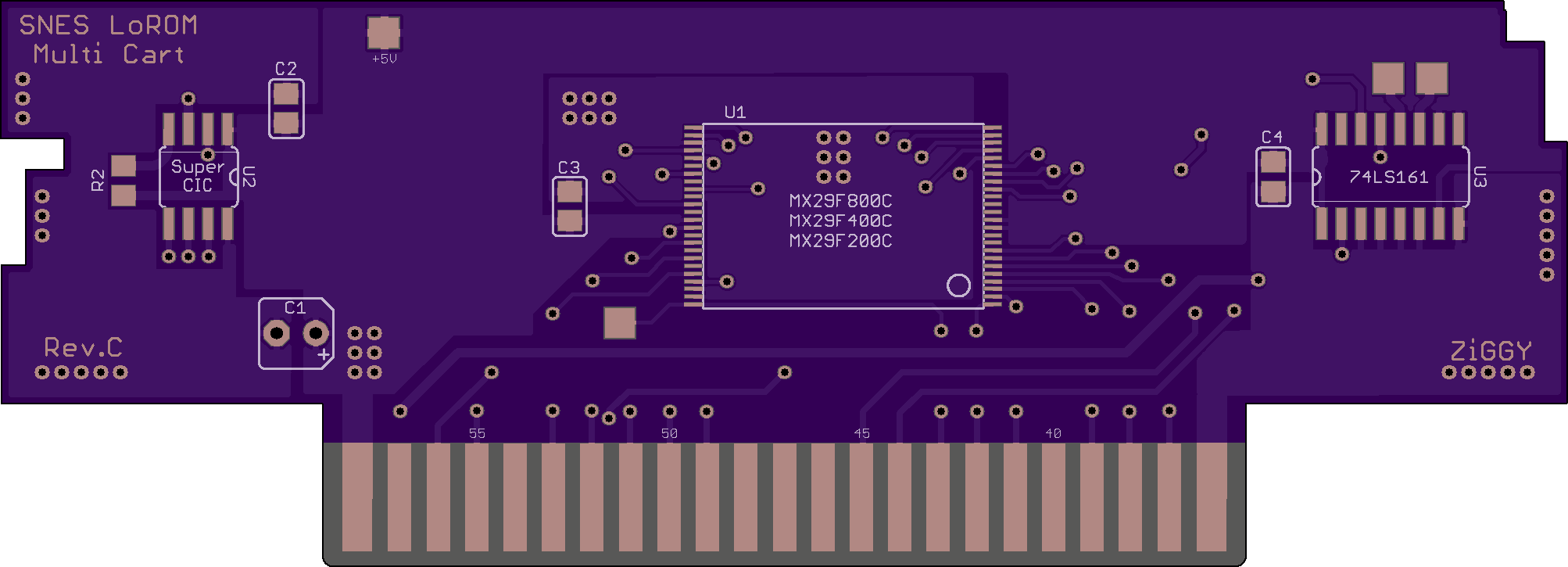
2 layer board of 4.01 x 1.45 inches (101.9 x 36.9 mm)
Uploaded:
March 03, 2018
Shared:
March 03, 2018
Total Price:
$29.10
NOTE: Rev.C is untested, but nothing dramatic has changed since Rev.B, mostly just cosmetic stuff. I’ll add a changelog at the bottom.
Description
You can use this PCB as a basic LoROM board with a max ROM size of 8Mib. Or, with the 74'161 installed, you can use this board as a 2-in-1 or 4-in-1 multi cart. Games are switched by hitting the console reset button.
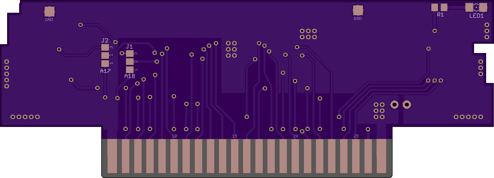
Jumper Settings
There are jumpers for the A18 and A17 address lines (JP1 and JP2) that will have to be set depending on how many games will be on the cart and what size memory you are using. For either jumper, closing positions 1 and 2 will allow the console to control that address line. Closing positions 2 and 3 will allow the 161 to control that address line. View the tables below to see how to set the jumpers when using 29F800 or 29F400 memory.
| No. Of Games (Memory = 29F800) | JP1 | JP2 |
|---|---|---|
| ONE | 1-2 | 1-2 |
| TWO | 2-3 | 1-2 |
| FOUR | 2-3 | 2-3 |
| No. Of Games (Memory = 29F400) | JP1 | JP2 |
|---|---|---|
| ONE | X | 1-2 |
| TWO | X | 2-3 |
BOM
| Part | Value | Package |
|---|---|---|
| U1 | MX29F800C | 48-TSOP |
| U1 | MX29F400C | 48-TSOP |
| U1 | MX29F200C | 48-TSOP |
| U2 ♥ | PIC12F629 | 8-SOIC |
| U3 ♦ | 74HC161D | 16-SOIC |
| C1 | 22 µF | Through Hole |
| C2 ♥ / C3 / C4 ♦ | 0.1µF | 0805 |
| JP1 ♠ / JP2 ♠ | 0 ohm | 0805 |
| R2 ♥ | 10 k ohm | 0805 |
Notes
♥ Use the SuperCIC key, found here. If your SNES is modified to deactivate the lockout chip, then you can omit this part if you wish. If you do not use the Super CIC, then do not populate C2 or R2. R2 is a pull-up resistor, the value isn’t crucial.
♦ If you are only installing one game on the cart, leave U3 and C4 unpopulated.
♣ R1 value is determined by the LED that you use. If you do not use an LED, you can leave R1 unpopulated.
♠ Jumper pads are spaced for 0 ohm 0805 resistors, but you can simply use a blob of solder instead. Alternatively, you can use a bit of wire or the trimmed legs from C1.
☼ LED is 1206 package to make it easy if you do not wish to use a surface mount LED. You can use wire or the legs of a through hole LED instead.
☼ DO NOT order this board with OSH Park’s standard 1.6mm board thickness. 1.6mm is too thick and you wont be able to insert the cart in the console (you will likely damage your cart slot if you somehow manage). Correct board thickness for SNES carts should be 1.2mm, which OSH Park does not currently offer.
Changelog
Rev.C
- Fixed J1 and J2 mirrored silkscreen labels, cleaned up silkscreen identifiers
- Moved C1 further away from U2, amended GND and +5V planes
- Moved via for U3 pin 14 further from U3
- Changed J3 to R2 (disables SuperCIC pair mode)
- Added solder pad for U3 pin 11 (QD), added extra GND pad
Rev.B
- Added additional silkscreen identifiers
- Added solder pad for U1 pin 48 (A16)
- Added solder pad for U3 pin 12 (QC)
NOTE: Rev.C is untested, but nothing dramatic has changed since Rev.B, mostly just cosmetic stuff. I’ll add a changelog at the bottom.
Description
You can use this PCB as a basic LoROM board with a max ROM size of 8Mib. Or, with the 74'161 installed, you can use this board as a 2-in-1 or 4-in-1 multi cart. Games are switched by hitting the console reset button.
Jumper Settings
There are jumpers for the A18 and A17 address lines (JP1 and JP2) that will have to be set depending on how many games will be on the cart and what size memory you are using. For either jumper, closing positions 1 and 2 will allow the console to control that address line. Closing positions 2 and 3 will allow the 161 to control that address line. View the tables below to see how to set the jumpers when using 29F800 or 29F400 memory.
| No. Of Games (Memory = 29F800) | JP1 | JP2 |
|---|---|---|
| ONE | 1-2 | 1-2 |
| TWO | 2-3 | 1-2 |
| FOUR | 2-3 | 2-3 |
| No. Of Games (Memory = 29F400) | JP1 | JP2 |
|---|---|---|
| ONE | X | 1-2 |
| TWO | X | 2-3 |
BOM
| Part | Value | Package |
|---|---|---|
| U1 | MX29F800C | 48-TSOP |
| U1 | MX29F400C | 48-TSOP |
| U1 | MX29F200C | 48-TSOP |
| U2 ♥ | PIC12F629 | 8-SOIC |
| U3 ♦ | 74HC161D | 16-SOIC |
| C1 | 22 µF | Through Hole |
| C2 ♥ / C3 / C4 ♦ | 0.1µF | 0805 |
| JP1 ♠ / JP2 ♠ | 0 ohm | 0805 |
| R2 ♥ | 10 k ohm | 0805 |
Notes
♥ Use the SuperCIC key, found here. If your SNES is modified to deactivate the lockout chip, then you can omit this part if you wish. If you do not use the Super CIC, then do not populate C2 or R2. R2 is a pull-up resistor, the value isn’t crucial.
♦ If you are only installing one game on the cart, leave U3 and C4 unpopulated.
♣ R1 value is determined by the LED that you use. If you do not use an LED, you can leave R1 unpopulated.
♠ Jumper pads are spaced for 0 ohm 0805 resistors, but you can simply use a blob of solder instead. Alternatively, you can use a bit of wire or the trimmed legs from C1.
☼ LED is 1206 package to make it easy if you do not wish to use a surface mount LED. You can use wire or the legs of a through hole LED instead.
☼ DO NOT order this board with OSH Park’s standard 1.6mm board thickness. 1.6mm is too thick and you wont be able to insert the cart in the console (you will likely damage your cart slot if you somehow manage). Correct board thickness for SNES carts should be 1.2mm, which OSH Park does not currently offer.
Changelog
Rev.C
- Fixed J1 and J2 mirrored silkscreen labels, cleaned up silkscreen identifiers
- Moved C1 further away from U2, amended GND and +5V planes
- Moved via for U3 pin 14 further from U3
- Changed J3 to R2 (disables SuperCIC pair mode)
- Added solder pad for U3 pin 11 (QD), added extra GND pad
Rev.B
- Added additional silkscreen identifiers
- Added solder pad for U1 pin 48 (A16)
- Added solder pad for U3 pin 12 (QC)
