Conductance monitor, real-time graph plotting, extremely high sensitivity and range ("Quantum Entanglement GWAAMC Aid v1.0") for Arduino UNO-type MCUs combined into a single file
author: kenneth558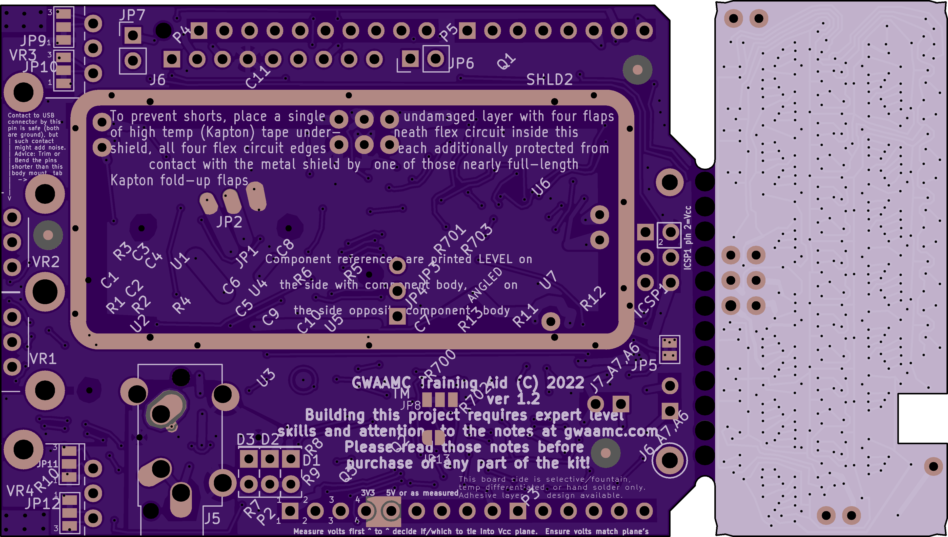
2 layer board of 3.74 x 2.12 inches (95.0 x 53.8 mm)
Uploaded:
December 09, 2022
Shared:
December 09, 2022
Total Price:
$39.60
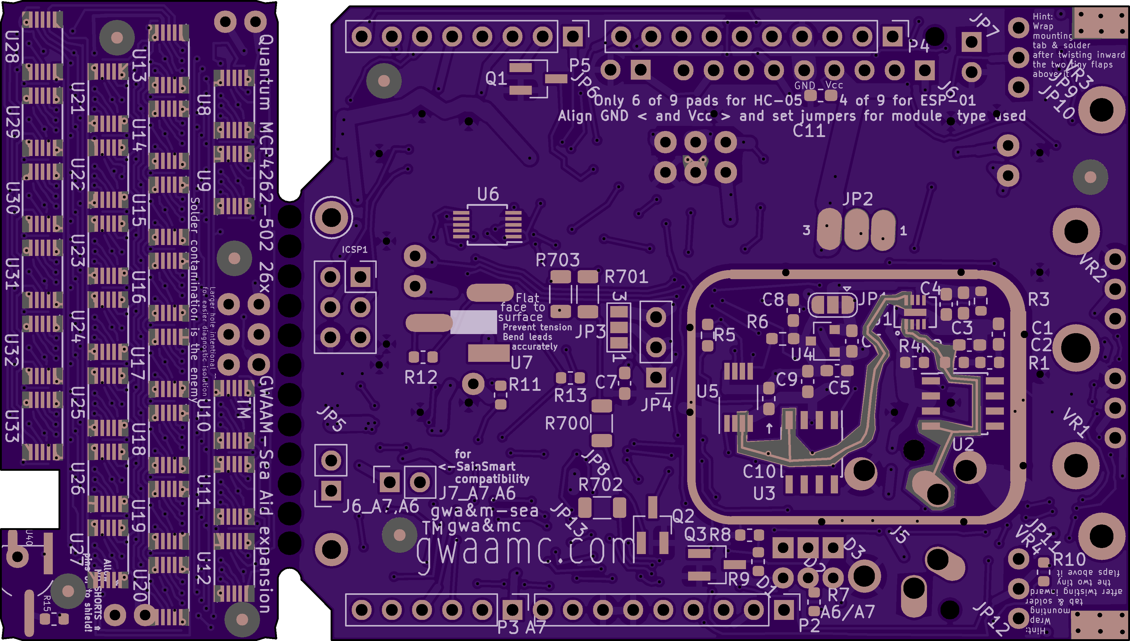
Same as two-file version [removed until revised], but here you can keep both boards attached until components are all placed and tests are successful. Circuit testing while boards are attached will require air-wiring to complete 11 connections - which ones should be obvious to you. Pick and place fiducials included in case you decide to contract the soldering to a pick and place fabricator. Order in 2oz copper to reduce risk of ENIG pads delaminating from the double-tinning required in ENIG. Solder paste stencil files located here.
Uses the plotter in the Arduino IDE to observe changes in electrical conductance that occur in plant tissue in vivo and in situ. The intended stimulus to produce said conductance response can be called telepathically transmitted empathy (telempathy), but a more religious term for it is very close to “faith”. By changing electrode types and DUT to your own preferences, this may be used in numerous other ways as well. It is designed for extreme sensitivity applications if you follow the instructions in making the shield hermetically sealed and keep the PCB from contamination indefinitely. This device is capable of detecting nano-ampere changes driving a high impedance DUT. Its current drive is limited to about 10 mA if R5 is bypassed (shorted out), but the value of R5 in the given design limits current to a few microAmps, consistent with the intended application.
Observing anything, even a plant, that is producing a voltage (as in Plant Electrophysiology) is not supported. Using this device for Plant Electrophysiology will combine both the voltage and conductive aspects of the DUT into something indecipherable relative to the intended purpose. There is a completely different product for Plant Electrophysiology called Plant SpikerBox (that has been confused with this GWAAMC project) which observes only the voltages produces by certain plants that respond physically to physical-dimension stimuli. That product does not apply the electrical current to the DUT required to observe conductance.
This GWAAMC device does apply current, but it will also be affected by voltages produced by the DUT because those voltages will affect the resultant current. The claim being investigated by this GWAAMC device is that non-physical dimension interactions can cause plants to respond with a change in their electrical conductance rather than them responding with voltage. The claim by those investigating in the Plant Electrophysiology field is that some plants produce a voltage response to physical dimension stimuli - not all that unexpected nor exciting, I’d say, even though it is a fairly new field of study, to be sure.
Uses UNO A6 and A7 (ADC6 & ADC7) that the advanced UNO boards have started including on J2 pins 1 and 9 (BaiTe, CNEWTEC) and an additional connector that SainSmart uses. (mating some pins may require reflowing angled ones) Provides for wireless which is not in the BOM nor in the sketch - you’ll have to shop for that and use/program it without our help right now. That footprint follows the HC-05 convention. With the Arduino 101 which uses its own BLE wireless, the HC-05 footprint can be used with a wifi device of the same pinout as a HC-05 so you can have two different wireless means of communication IF YOU MAKE SKETCH CHANGES TO DO SO. (As you read my surmisings following relative to 3.3V operation, remember that I have NOT proved 3.3V operation)
If using this with Arduino 101 or for some other reason 3.3V appears on ICSP1 pin 2 of your MCU, follow instructions for J2 pins 4 and 5 jumpering with solder and wire or pin from pin 5. If your MCU operates at 3.3V but 5V appears on your MCU ICSP1 pin 2 (I’m thinking of Arduino Zero), you’ll also have to remove one side or the other of ICSP1 pin 2 to keep from shorting 3.3V to 5V. Note that power will then only be reaching this board through a single pin instead of 2 pins, nearly doubling whatever voltage drop there is between the two boards. Hopefully that extra voltage drop will be insignificant, but then again, it may prevent the HC-05 type wireless module from working. When I determine how to make it work as good at 3.3V as it does at 5V the following 2 notes will be apropos -
Modifying for 3V will mean you cannot then use in 5V environment unless the mod is unsoldered and reversed, since I didn’t find room on the board there for a slide-on/off jumper. However, if you don’t mind a sliding jumper dangling off the edge of the board, you might be able to fashion such a jumper for easier interchangeability between 5V and 3V systems.
Note that in 3V systems, Q1 and Q2 MAY need to be shorted across D-S, which would reduce sensitivity an unknown amount. Until I get things working in a 3V3 environment, I won’t know specifics any better than that.
If your soldering skill set is from repair like mine is, you could be in for a surprise soldering onto a new board - whatever plating you ordered on the pad leaches into the solder you apply and instantly causes its melting point to increase 10-20 degrees from bare naked solder, un-wetting the pad if you don’t have the temperature high enough to overcome it. It happens while you try to place each component onto new pads that are plated with any metal (like gold) or alloy (like a solder-ish tinning) dissimilar to the solder you’re using. In a word, your solder becomes less eutectic by cross contamination with whatever the fab house plated the pad with. Additionally, gold and lead do not play well together in solder (“embrittlement”), and neither does lead and bismuth (fail by SnPbBi)…double tinning is the fix to wash gold plate off, no remedy is available for the PbBi contamination. That one sure blindsided me.
To achieve a hermetic seal around the shields that U4 requires, SnBi solder is recommended in the specific vias due to that solder expanding on solidifying to give a good seal. Being a low MP solder, this implies you would seal the specific vias after higher MP soldering is completed. You might ask which vias are the “specific” ones. They are about 12 in number that could vent ambient air into any shield.
Inspired by the deeds and words of our Lord Jesus Christ when He made the fig tree wither overnight with a curse and by the findings of Cleve Backster using the GSR aspect of a polygraph machine. The details found at http://gwaamc.com should be consulted for further info before deciding to build this yourself. You’ll also find the BOM there. Note that ordering with the gerbers at gwaamc.com will not only ensure you have the most advanced version of this training aid available, but allow you to order from any fab house you choose.
