Giuglio LED Shifter
author: Frederic-Maria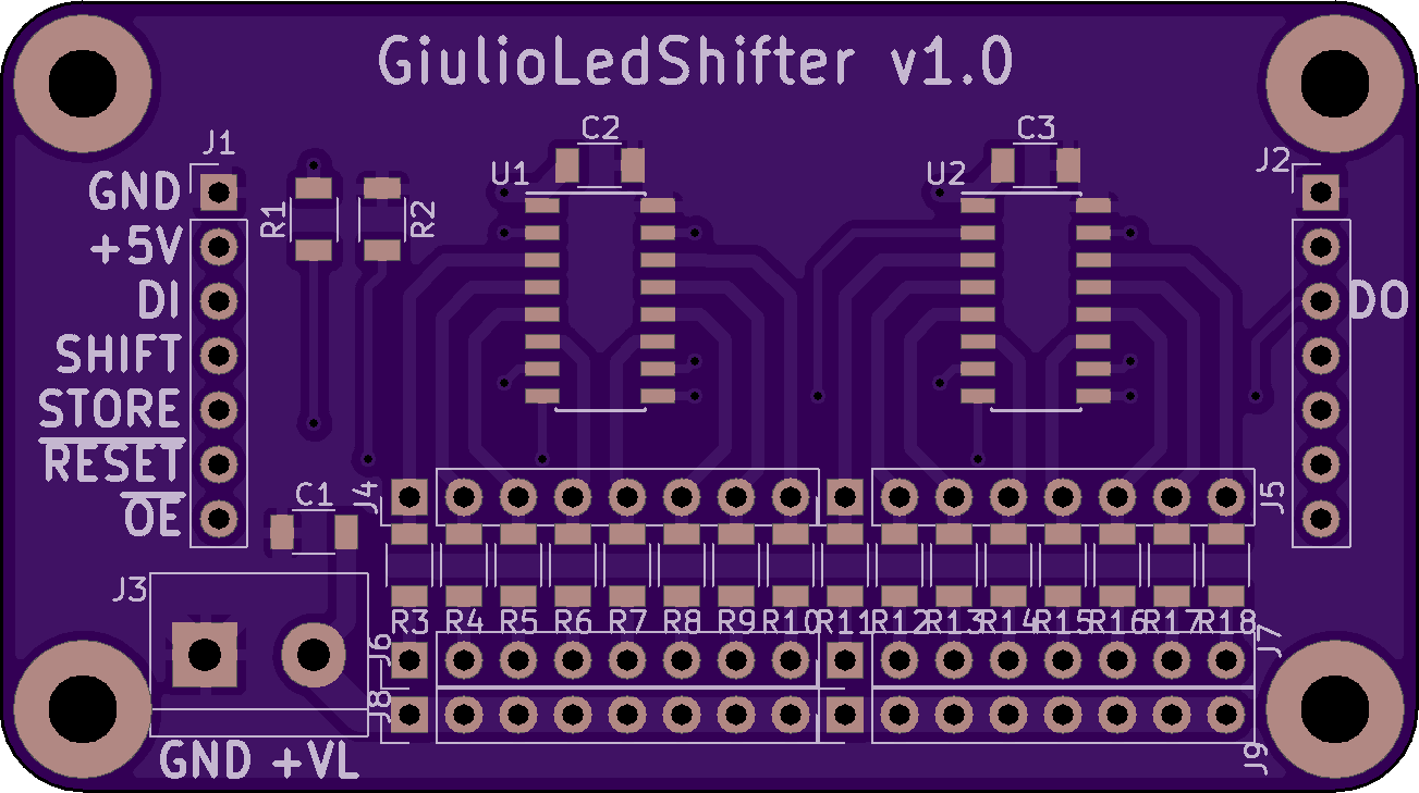
2 layer board of 2.61 x 1.46 inches (66.2 x 37.0 mm)
Uploaded:
March 04, 2018
Shared:
December 26, 2018
Total Price:
$18.95
This module offers 16 open drain outputs. It is based on the NPIC6C595 shift register. Many modules can be chained together to increase the number of outputs.
How to use
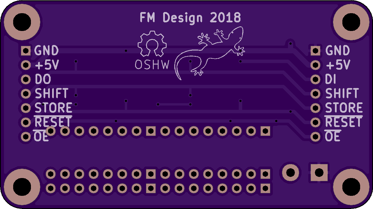
Use the J1 connector to provide input to the module. J2 connector is meant as an output connector to be connected to an extra chained module- the DO output (J2) is connected to the DI input (J1) of the chained module.
Inputs DI, SHIFT and STORE allow shifting data into the registers. DI - the data input - must be set before creating a pulse on SHIFT input to shift the data value by one bit. Once all bits have been shifted, create a pulse on STORE input to really get all the bits available at ouput.
Input /RESET and /OE may not be connected to a micro-controller, in such a case, resistors R1 and R2 can be used to pull /RESET and /OE signals to +5V and GND respectively (no reset, output enabled).
Outputs can be used to drive LEDs or relays, up to 100mA per output - see NPIC6C595 datasheet.
Connector J3 provides power input. GND is common with GND on J1 and J2. +VL is dispatched to J8-J9.
Resistors R3-R18 can be used to limit output current in case of LED connected between J6-J7 and J8-J9. If no need to use resistors, connectors J4-J5 can be used directly instead of J6-J7.
It is up to you to decide wether you have to use J8-J9 to dispatch +VL to LEDs.
Output power supply
Up to 1.6 amps can be necessary par card on the GND and +VL pins of the input power connector. So use adequate power supply and cables.
+VL can be up to 33V as per datasheet.
Bill of materials
| Reference | Device |
|---|---|
| U1, U2 | NPIC6C595 |
| C1, C2 | 1µF |
| R1, R2 | 22kΩ |
| R3-R18 | Depending on application |
This module offers 16 open drain outputs. It is based on the NPIC6C595 shift register. Many modules can be chained together to increase the number of outputs.
How to use
Use the J1 connector to provide input to the module. J2 connector is meant as an output connector to be connected to an extra chained module- the DO output (J2) is connected to the DI input (J1) of the chained module.
Inputs DI, SHIFT and STORE allow shifting data into the registers. DI - the data input - must be set before creating a pulse on SHIFT input to shift the data value by one bit. Once all bits have been shifted, create a pulse on STORE input to really get all the bits available at ouput.
Input /RESET and /OE may not be connected to a micro-controller, in such a case, resistors R1 and R2 can be used to pull /RESET and /OE signals to +5V and GND respectively (no reset, output enabled).
Outputs can be used to drive LEDs or relays, up to 100mA per output - see NPIC6C595 datasheet.
Connector J3 provides power input. GND is common with GND on J1 and J2. +VL is dispatched to J8-J9.
Resistors R3-R18 can be used to limit output current in case of LED connected between J6-J7 and J8-J9. If no need to use resistors, connectors J4-J5 can be used directly instead of J6-J7.
It is up to you to decide wether you have to use J8-J9 to dispatch +VL to LEDs.
Output power supply
Up to 1.6 amps can be necessary par card on the GND and +VL pins of the input power connector. So use adequate power supply and cables.
+VL can be up to 33V as per datasheet.
Bill of materials
| Reference | Device |
|---|---|
| U1, U2 | NPIC6C595 |
| C1, C2 | 1µF |
| R1, R2 | 22kΩ |
| R3-R18 | Depending on application |
