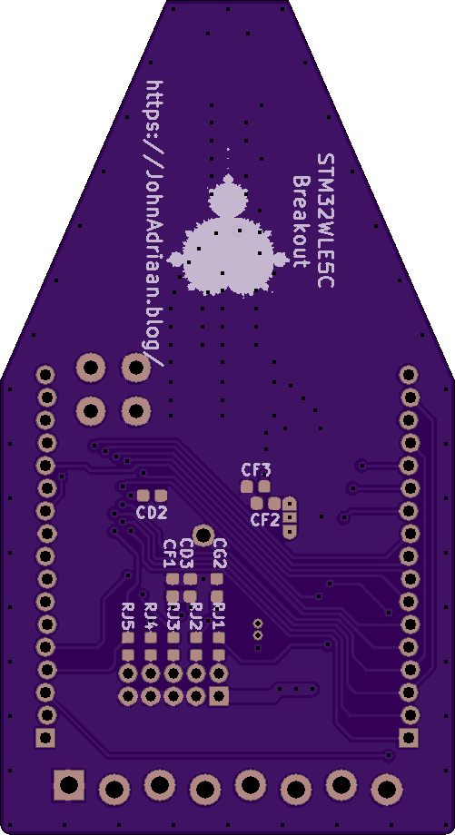
STM32WLE5C Breakout
author: JohnAdriaan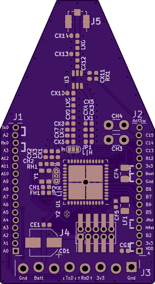
4 layer board of 1.00 x 1.84 inches (25.5 x 46.8 mm)
Uploaded:
September 21, 2020
Shared:
September 21, 2020
Total Price:
$18.40
ST Micro produced a great new chip! And then they packaged it inside a 9x9 0.5mm BGA… I tried to produce a PCB for it, but the limits were too great (tiny?) for OSHPark.
And then ST announced two more packages - and one wasn’t a BGA! It has fewer pins, and isn’t available yet, but this time I could stay within OSHPark’s parameters.
This board gives a breakout for all the GPIO pins (except see below), as well as components for all the special purpose sections. Note, however, the board has not been tested! I will be posting the schematic and BOM soon!
Features
Apart from the actual STM32WLE5C chip, this board has the following features:
- The board is tiny! It is designed to be used standalone, or as a module for a larger board (uploaded soon!).
- The antenna is attached via a U.FL connector.
- The 32 MHz TCXO and support components are included, and wired to
PB0(sorry, not available on a header). - The PE4259 RF switch and RF signal path components are included.
- Both Low and High TX power paths are supported with solder jumpers
JP1andJP2- one MUST be chosen and soldered before powering on! - There’s an FTDI header (with extra pins for Battery), although it only supports 3v3 instead of 5v. Note that the linked device only supports 50mA, which is fine unless you’re using TX/PA High!
- The GPIO breakout is to 2× 17-pin 0.05" headers, for GPIOs and special pins:
- Port A is on its own header, assigned to the correct pin numbers (starting at pin
0). There are also jumpers to connect to the FTDI RxD and TxD; - Ports B and C are on a second header, also assigned to the correct pin numbers - they coincidentally(?) interleave!
- Special purpose pins are brought out, and are next to relevant pins for easy jumpering:
BOOT0is next toGND(recommended) and3v3;Battis available for the Real Time Clock;NRSTis available, and next toJTRSTfor jumpering if desired (not necessary);VDDAis next to3v3, or can be connected to a separate supply if desired;PC14andPC15are brought out directly - but have PTH footprints for a 32.768kHz crystal and capacitors if desired (note that the long trace lengths will affect the capacitance required);AntSwCTRL for the PE4259 is available - connect to any GPIO.
- JTAG / SWD is brought out to a CS10 CoreSight connector - SMD, PTH and Pogo footprints are overlaid.
Thus the board can:
- Be programmed standalone by Pogo;
- Have an SMD or PTH connector soldered on for development work;
- Be fitted to a larger breakout board, with (more usable) 0.1" headers and STLink serial programmer.
- Port A is on its own header, assigned to the correct pin numbers (starting at pin
