PCB Test Swatch
author: joem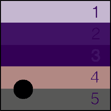

2 layer board of 0.72 x 0.72 inches (18.2 x 18.2 mm)
Uploaded:
May 10, 2020
Shared:
May 10, 2020
Total Price:
$2.55
A small (inexpensive) 0.72 x 0.72 inches (0.52 in2) sample that shows different layers possible when making a PCB. The numbered layers are as follows:
- Silkscreen on solder mask on copper
- Solder mask on copper
- Solder mask
- Copper
- Nothing (bare PCB)
And on the back there is a copper pour and a silkscreen fill (which overlap) running vertically so you can test possible translucency with the other side’s layers. Additionally, you should be able to write with permanent marker on the rear silkscreen fill to label where your sample came from.
(Depending on the manufacturer and the processes, some layers may not appear different from others on the final product.)
There is a project page on github for this with KiCad source files and gerbers.
Render from KiCad:
