Atari 130XE 320K Upgrade v2.2.kicad_pcb
author: Waynetho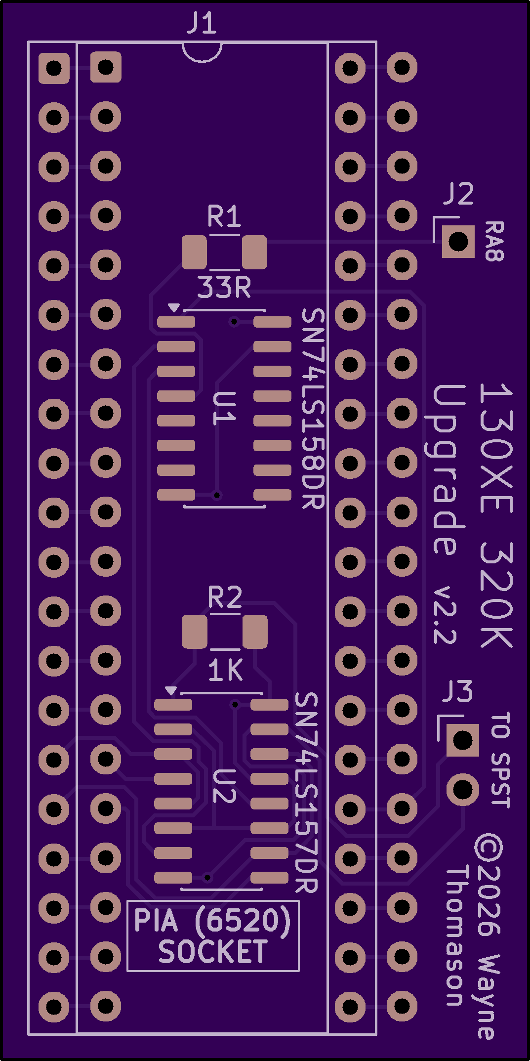
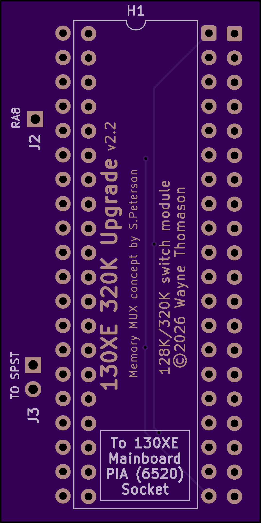
2 layer board of 1.07 x 2.14 inches (27.1 x 54.4 mm)
Uploaded:
September 11, 2026
Shared:
September 11, 2026
Total Price:
$11.40
320K upgrade for 130XE (or 16-chip 65XE upgraded to 130XE). Resides under the PIA (6520) chip on the mainboard. One connection to extended DRAM pin-1, two-pin connection to SPST switch, to toggle between stock 128K with ANTIC bank support and 320K. (Memory MUX concept by Scott Peterson)
Assemble in the following order:
Install SMT parts
Install and solder 20-pin turned pin header strip on back of board for pins 1-20. You may want to use a socket or breadboard and both header strips while soldering to ensure alignment. Only solder pins 1-20.
Clip the pins short.
Install and solder 40-pin socket on top.
Install and solder second 20-pin header strip for pins 21-40 using same alignment method used previously.
Install and solder J2 and J3 horizontal headers.
NOTE: Do not use wide SMT ICs with NSR suffix. Use only narrow ICs such as SN74LS158DR and SN74LS157DR.
Installation:
Assemble board
Desolder eight xx64 DRAM chips (i.e., MT4164, M3764) on the right bank of RAM (extended).
Install and solder the eight 16-pin sockets where DRAM was removed
Using hookup wire, connect pin-1 of all eight DRAM sockets together.
Insert and solder new 41256 DRAM chips in sockets
Desolder the PIA chip, 6520 - take care not to damage the chip
Install and solder 40-pin socket in mainboard where PIA was removed
Install upgrade board in PIA socket
Install PIA into upgrade board
Connect single-pin Dupont wire to J2 and run to opposite side of board and solder to one of the Socket pins that you previously connected with the hookup wire.
Cut the 2-pin Dupont wire to about 4-5" and attach and solder the cut end to SPST switch
Plug 2-pin Dupont connector into J3
Mount SPST switch in suitable location in the 130XE case
320K upgrade for 130XE (or 16-chip 65XE upgraded to 130XE). Resides under the PIA (6520) chip on the mainboard. One connection to extended DRAM pin-1, two-pin connection to SPST switch, to toggle between stock 128K with ANTIC bank support and 320K. (Memory MUX concept by Scott Peterson)
Assemble in the following order:
Install SMT parts
Install and solder 20-pin turned pin header strip on back of board for pins 1-20. You may want to use a socket or breadboard and both header strips while soldering to ensure alignment. Only solder pins 1-20.
Clip the pins short.
Install and solder 40-pin socket on top.
Install and solder second 20-pin header strip for pins 21-40 using same alignment method used previously.
Install and solder J2 and J3 horizontal headers.
NOTE: Do not use wide SMT ICs with NSR suffix. Use only narrow ICs such as SN74LS158DR and SN74LS157DR.
Installation:
Assemble board
Desolder eight xx64 DRAM chips (i.e., MT4164, M3764) on the right bank of RAM (extended).
Install and solder the eight 16-pin sockets where DRAM was removed
Using hookup wire, connect pin-1 of all eight DRAM sockets together.
Insert and solder new 41256 DRAM chips in sockets
Desolder the PIA chip, 6520 - take care not to damage the chip
Install and solder 40-pin socket in mainboard where PIA was removed
Install upgrade board in PIA socket
Install PIA into upgrade board
Connect single-pin Dupont wire to J2 and run to opposite side of board and solder to one of the Socket pins that you previously connected with the hookup wire.
Cut the 2-pin Dupont wire to about 4-5" and attach and solder the cut end to SPST switch
Plug 2-pin Dupont connector into J3
Mount SPST switch in suitable location in the 130XE case
