balanced amp.kicad_pcb
2 layer board of 1.00 x 1.40 inches (25.4 x 35.6 mm)
Uploaded:
October 18, 2019
Shared:
October 22, 2019
Total Price:
$7.00
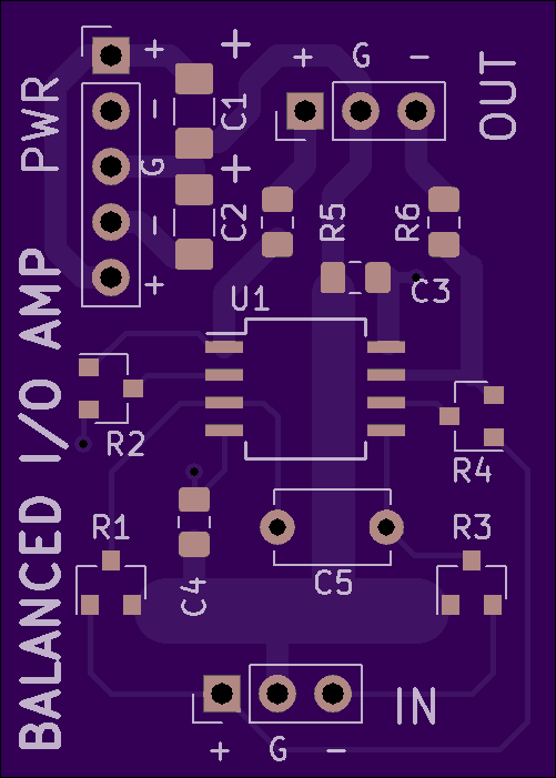
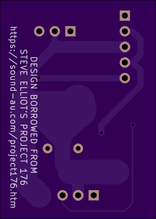
Derived from a Rod Elliott design (https://sound-au.com/project176.htm). A fully balanced, full differential audio amplifier. U1 is an NE5532 but is a universal dual op amp footprint if you want to use something else. Connectors are standard 0.1" headers or wire directly onto the board with the p…
Show full description
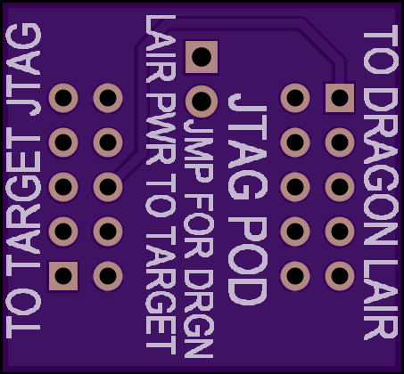
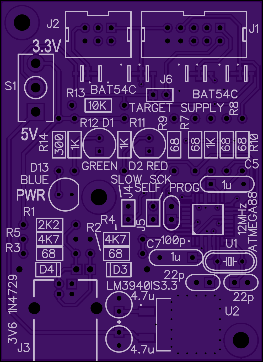
DRAGON LAIR JTAG CABLE POD
2 layer board of 0.91 x 0.84 inches (23.0 x 21.4 mm)
Uploaded:
September 13, 2015
Shared:
October 13, 2015
Total Price:
$3.80
Descrambler for Dragon Lair JTAG output at Target end of JTAG cable.
This is to be used with Dragon Lair #2 buffer board on my projects page here at OSHPark. Th basic schematic of this can be found at: http://n1.taur.dk/permanent/dragonhide.pdf I added a jumper to optionally disconnect power…
Show full description
9XTX CONTROLLER
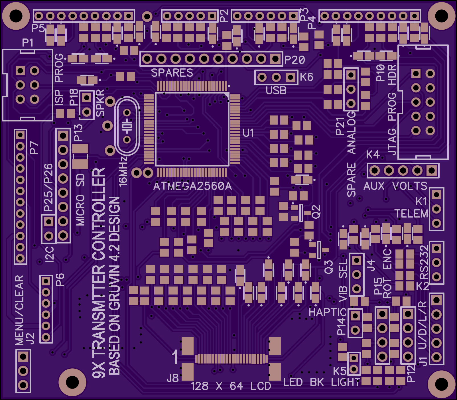

4 layer board of 3.21 x 2.81 inches (81.4 x 71.3 mm)
Uploaded:
September 04, 2015
Shared:
September 04, 2015
Total Price:
$89.90
A 9X RC transmitter controller based on the Gruvin9X 4.2 design using an ATMEGA2560 MCU. This is a 4 layer ultra compact design to be retrofitted into almost any reasonably sized non-Turnigy/FlySky case. All 4 layers have copper planes for voltages and ground including a portion for Analog Groun…
Show full description
Dragon Lair #2
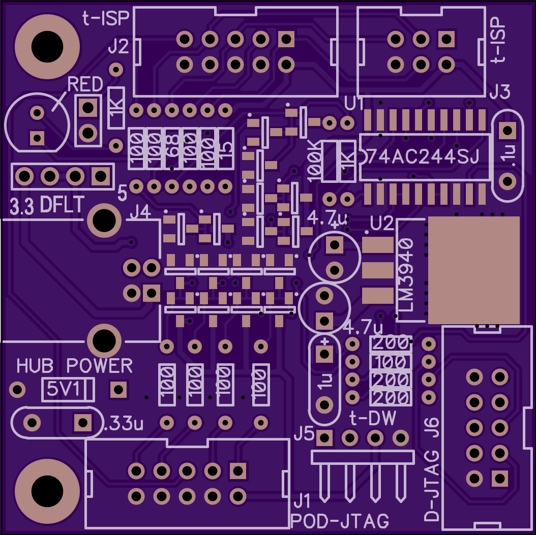

2 layer board of 2.11 x 2.11 inches (53.5 x 53.5 mm)
Uploaded:
August 30, 2015
Shared:
September 04, 2015
Total Price:
$22.15
This is a rendition of the Dragon Lair board by Nard at: http://www.aplomb.nl/TechStuff/Dragon/Dragon.html
The POD-JTAG connector, J1, is not pinned out for standard JTAG pin sequence but is based on the improved signal integrity pin out as described by Kasper (KKP) in this document: http://n1…
Show full description
AVR USBASP_PROGRAMMER V1.0
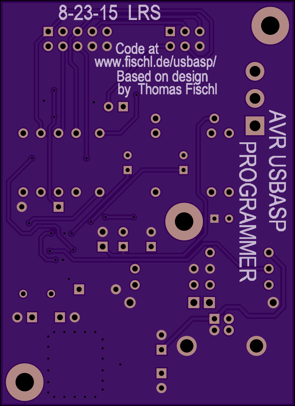
2 layer board of 2.01 x 2.76 inches (51.0 x 70.0 mm)
Uploaded:
August 24, 2015
Shared:
August 24, 2015
Total Price:
$27.60
A version of the classic Atmel ISP programmer by Thomas Fischl. This one supports 3.3V and 5V operation on the Programmer and Target and has Schottky ESD protection diodes on the 4 main lines for the ISP. A Low drop out regulator makes 3.3V from the 5V USB supplied voltage. Both 6 and 10 pin hea…
Show full description
